
Signal Processing
Index 34
VERY LOW POWER GATED CRYSTAL OSCILLATORS
Published:2012/11/9 0:03:00 Author:muriel | Keyword: VERY LOW POWER , GATED CRYSTAL OSCILLATORS

The circuit gates the output of a continuously operating 32KHz crystal oscillator to the input of a C-MOS buffer when clock pulses are needed. The technique gets around the problem of a slow starting crystal oscillator by keeping the oscillator going and switching on a transistor power stage only as needed. The method keeps the standby power consumption to a very low 1uA when used with a 3v supply. (View)
View full Circuit Diagram | Comments | Reading(1252)
VERY LOW POWER ASTABLE MULTIVIBRATOR
Published:2012/11/9 0:01:00 Author:muriel | Keyword: VERY LOW POWER , ASTABLE MULTIVIBRATOR
This classic circuit draws only 200 nanoamps from a 1.5v supply.
(View)
View full Circuit Diagram | Comments | Reading(1896)
ULTRA PURE 125KHz SINE WAVE SIGNAL SOURCE
Published:2012/11/9 Author:muriel | Keyword: ULTRA PURE , 125KHz , SINE WAVE SIGNAL SOURCE
For some RFID systems operating at 125KHz, a very low distortion signal source reference is needed. The circuit shown on this page produces a 10-volt peak-to-peak signal into a 50-ohm load, with a distortion of only 0.01%.
(View)
View full Circuit Diagram | Comments | Reading(2124)
MEDIUM POWER 125KHZ OSCILLATOR-2
Published:2012/11/8 1:36:00 Author:muriel | Keyword: MEDIUM POWER , 125KHZ, OSCILLATOR-2
View full Circuit Diagram | Comments | Reading(1331)
MEDIUM POWER 125KHZ OSCILLATORS
Published:2012/11/8 1:35:00 Author:muriel | Keyword: MEDIUM POWER, 125KHZ OSCILLATORS
View full Circuit Diagram | Comments | Reading(1122)
300-V PEAK TO PEAK SIGNAL GENERATOR
Published:2012/11/8 1:13:00 Author:muriel | Keyword: 300-V, PEAK TO PEAK , SIGNAL GENERATOR
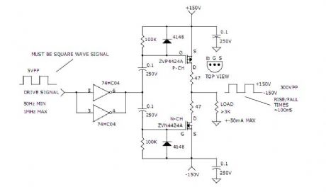
View full Circuit Diagram | Comments | Reading(1051)
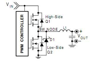
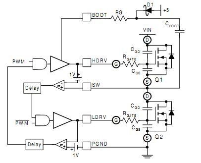
AN-6005 synchronous buck circuit
Published:2012/10/30 22:29:00 Author:muriel | Keyword: AN-6005, synchronous buck circuit
View full Circuit Diagram | Comments | Reading(887)
AN-6003 synchronous buck circuit
Published:2012/10/30 22:27:00 Author:muriel | Keyword: AN-6003 , synchronous buck circuit
View full Circuit Diagram | Comments | Reading(810)
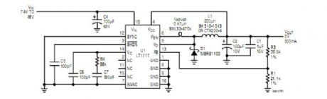
100kHz Low Noise Step-Down Switching Regulator
Published:2012/10/30 22:06:00 Author:muriel | Keyword: 100kHz, Low Noise, Step-Down Switching Regulator
View full Circuit Diagram | Comments | Reading(732)
The oscillator and trigger circuit with operational amplifier
Published:2012/10/29 21:34:00 Author:Ecco | Keyword: oscillator , trigger , operational amplifier
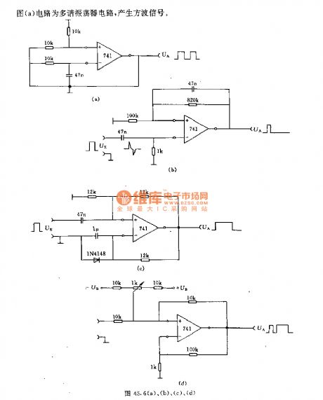
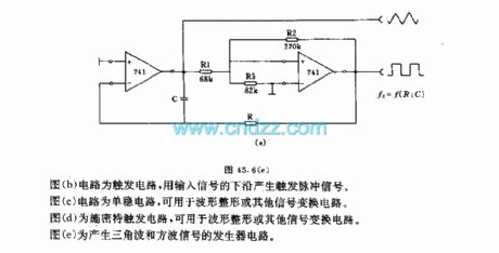
Fig a shows a multivibrator circuit which can generate square wave signal; Figure b is a flip-flop circuit which uses the under edge of the input signal to generate a trigger pulse signal. Figure c is a monostable circuit which can be used for waveform shaping or other signal conversion circuits. Figure d shows a Schmitt trigger circuit for waveform shaping or other signal conversion circuit. Figure e is a triangle wave and square-wave signal generator circuit.
(View)
View full Circuit Diagram | Comments | Reading(2115)
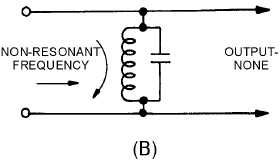
Highpass filters
Published:2012/10/29 1:44:00 Author:muriel | Keyword: Highpass filters
View full Circuit Diagram | Comments | Reading(784)
3-Band Equalizer
Published:2012/10/29 1:42:00 Author:muriel | Keyword: 3-Band Equalizer
View full Circuit Diagram | Comments | Reading(0)
simple bandpass filter
Published:2012/10/25 20:49:00 Author:muriel | Keyword: simple, bandpass filter
View full Circuit Diagram | Comments | Reading(965)
Bandpass Filter
Published:2012/10/25 20:47:00 Author:muriel | Keyword: Bandpass Filter

This circuit is taken from the Progressive Communications Receiver in most of the recent ARRL Handbooks. Values for the 40 meter band are shown.
If you want the ultimate in a bandpass filter for 40 or 20 meters, check out the bandpass filters in An Integrated Contest-Grade CW Station , Solid State Design for the Radio Amateur, by Wes Hayward and Doug DeMaw, Page 225. (View)
View full Circuit Diagram | Comments | Reading(3113)
Buffer Stage. One Per Output Needed
Published:2012/10/25 3:13:00 Author:muriel | Keyword: Buffer, One Per Output

These buffers should use high quality opamps, and they are included on the PCB, including the trimpot (see the photo at the beginning of this article).
Several people (including me) have found that the crossover unit has a short 'chirp' or 'snap' (depending on the opamp characteristics) as power is removed, and this may be accompanied by some DC swing. If you use the new version of the P05B preamp power supply, the auxiliary output can be used to activate a 6-pole relay (or as many smaller relays as needed) to short all outputs to earth when there is no power. The normally closed contacts simply short the outputs to ground, and when power is applied the short is removed. P05 (Rev-B) boards have a power-on delay and a loss of AC detector that will mute the crossover for a few seconds at power-on, and almost immediately when power is turned off. (View)
View full Circuit Diagram | Comments | Reading(890)
Designing Our First Filter
Published:2012/10/25 2:35:00 Author:muriel | Keyword: Filter

The first active filter must be the first order low pass. By simply reversing the filter components, this becomes a first order high pass. In each case, the filter only consists of the resistance and capacitance, with the opamp simply isolating the filter from the following stages. Q is not variable in a first order filter, and the only options are high pass and low pass. A bandpass filter can only be created by cascading a high and low pass filter. Although the least useful of all filters, they are easy to understand, so make a good starting point. (View)
View full Circuit Diagram | Comments | Reading(785)
RC Notch Filter (Twin T)
Published:2012/10/23 20:23:00 Author:muriel | Keyword: RC Notch Filter , Twin T

The twin T notch filter can be used block an unwanted frequency or if placed around an op-amp as a bandpass filter. The notch frequency occurs where the capacitive reactance equals the resistance (Xc=R) and if the values are close, the attenuation can be very high and the notch frequency virtually eliminated. The insertion loss of the filter will depend on the load that is connected to the output, so the resistors should be of much lower value than the load for minimal loss. At audio frequencies, the filter could function as a bass and treble boost circuit by attenuating the mid range frequencies. Using 1.5K resistors and 0.1uF capacitors, the band stop at -10dB is about 500 Hz to 2Khz. The depth and width of the response can be adjusted somewhat with the 0.5R value and by adding some resistance across the C values. If the circuit is used around an op-amp as a bandpass filter, the response may need to be dampened to avoid oscillation. (View)
View full Circuit Diagram | Comments | Reading(1517)
Monostable Flip Flop
Published:2012/10/23 20:18:00 Author:muriel | Keyword: Monostable, Flip Flop
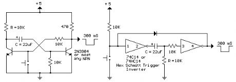
The monostable flip flop, sometimes called a 'one shot' is used to produce a single pulse each time it is triggered. It can be used to debounce a mechanical switch so that only one rising and one falling edge occurs for each switch closure, or to produce a delay for timing applications. In the discrete circuit, the left transistor normally conducts while the right side is turned off. Pressing the switch grounds the base of the conducting transistor causing it to turn off which causes the collector voltage to rise. As the collector voltage rises, the capacitor begins to charge through the base of the opposite transistor, causing it to switch on and produce a low state at the output. The low output state holds the left transistor off until the capacitor current falls below what is needed to keep the output stage saturated. When the output side begins to turn off, the rising voltage causes the left transistor to return to it's conducting state which lowers the voltage at it's collector and causes the capacitor to discharge through the 10K resistor (emitter to base). The circuit then remains in a stable state until the next input. The one shot circuit on the right employs two logic inverters which are connected by the timing capacitor. When the switch is closed or the input goes negative, the capacitor will charge through the resistor generating an initial high level at the input to the second inverter which produces a low output state. The low output state is connected back to the input through a diode which maintains a low input after the switch has opened until the voltage falls below 1/2 Vcc at pin 3 at which time the output and input return to a high state. The capacitor then discharges through the resistor (R) and the circuit remains in a stable state until the next input arrives. The 10K resistor in series with the inverter input (pin 3) reduces the discharge current through the input protection diodes. This resistor may not be needed with smaller capacitor values.
Note: These circuits are not re-triggerable and the output duration will be shorter than normal if the circuit is triggered before the timing capacitors have discharged which requires about the same amount of time as the output. For re-triggerable circuits, the 555 timer, or the 74123 (TTL), or the 74HC123 (CMOS) circuits can be used. (View)
View full Circuit Diagram | Comments | Reading(1447)
CMOS Toggle Flip Flop Using Laser Pointer
Published:2012/10/23 20:18:00 Author:muriel | Keyword: CMOS , Toggle , Flip Flop , Laser Pointer
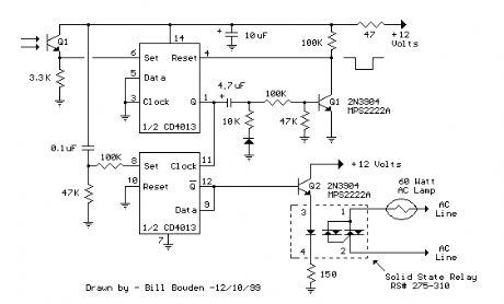
The circuit below is similar to the one above but can be used with a laser pointer to toggle the relay rather than a push button. The IR photo transistor Q1 (Radio Shack 276-145A) or similar is connected to the set input (pin 6). The photo transistor should be shielded from direct light so that the voltage at the set input (pin 6) is less than 1 volt under ambient conditions and moves to more than 10 volts when illuminated by the laser pointer or other light source. The reset time is about a half second using a 4.7uF cap which prevents the circuit from toggling more than once during a half second interval. The 10K resistor and diode provide a faster discharge path for the 4.7uF cap so the circuit can be retoggled in less than 1 second. The 3K resistor in series with the photo transistor may need be adjusted for best performance. The relay shown is a solid state variety to be used with lights or other resistive loads at less than 3 amps. A mechanical relay can also be used as shown in circuit above. (View)
View full Circuit Diagram | Comments | Reading(1058)
AM Radio Receiver With Additional IF Stage
Published:2012/10/22 21:55:00 Author:muriel | Keyword: AM Radio Receiver, Additional IF Stage
Pictured above is the same circuit with an additional IF stage added forgreater sensitivity. Overall gain can be adjusted with the 1K resistorsin the emitter leg of the 2N3904 transistors. The circuit board was assembledusing multiturn 10K pots in place of the 1K resistors and then adjusted forbest performance. The pots are the 2 little blue items just to the left ofthe tuning cap. I think I ended up with about 750 ohms. The emitter bypasscaps are not needed since there is plenty of gain available without them.The caps (two yellow items near the pots) are still in the board but notconnected. I didn't know if they were needed or not, so I put them in thereanyway and later disconnected them. Removing the bypass caps also increasesthe input impedance so that both IF stages can use the black IF coils whichhave higher secondary impedances (and thus more voltage) than the yellow orwhite coils. You might be able to replace the yellow coil with a black onefor greater signal transfer since the input to the first transistor is muchhigher without the bypass cap, but I didn't try it. You may notice one of theblack coils is actually white in the picture but it was rewound for a highersecondary impedance. Actually, it was removed from a junk radio purchased fora dollar and didn't have any secondary, so I added a 27 turn secondary whichis close to what the black coils use. Overall, the performance is very goodexcept for the AGC circuit, which has limited range and may not be ableto compensate for very strong stations which may overload the circuit.The AGC voltage is derived from the IF amplitude at the cathode of thedetector diode (output of T4). As the IF amplitude increases, the DCvoltage at the gate of the JFET will move negative, below ground.The audio signal is present on both the gate and source terminals of theJFET, but the audio DC offset voltage will change as the IF amplitudechanges. This DC voltage (about 2 volts) is fed back through a 15K resistorand the two IF coil secondaries to control the transistor bias points.The audio signal is filtered out by the 47uF cap leaving a stable DCvoltage at the base of the transistors. As the base voltage drops, theemitter voltages also drop resulting in less operating current and lowergain for two IF stages. But the range is limited to maybe only 6-12dBwhich isn't enough to compensate for very strong signals. One solutionto the problem is a manual gain control consisting of a switch anda few turns of wire around the antenna coil which can be seen in thepicture (3 turns of solid insulated white wire on left side of loopstick).Closing the switch loads the antenna coil and reduces the signal level. (View)
View full Circuit Diagram | Comments | Reading(2812)
| Pages:34/195 At 202122232425262728293031323334353637383940Under 20 |
Circuit Categories
power supply circuit
Amplifier Circuit
Basic Circuit
LED and Light Circuit
Sensor Circuit
Signal Processing
Electrical Equipment Circuit
Control Circuit
Remote Control Circuit
A/D-D/A Converter Circuit
Audio Circuit
Measuring and Test Circuit
Communication Circuit
Computer-Related Circuit
555 Circuit
Automotive Circuit
Repairing Circuit