
Signal Processing
Index 35
AM Radio Receiver Using the NE602 Balanced Mixer
Published:2012/10/22 21:54:00 Author:muriel | Keyword: AM Radio Receiver, NE602 , Balanced Mixer
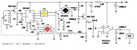
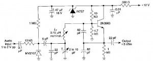
Pictured above is a little AM superhetrodyne receiver that covers thebroadcast band from 550 Khz to 1650 Khz. The circuit employs the 8 pinSignetics balanced mixer IC (NE602) which converts the incoming RF signalto the standard 455 Khz IF signal and provides about 13dB gain. The IFsignal is amplified by a single transistor stage and audio is recoveredusing a biased shotkey diode (5082) and JFET buffer transistor. The LM386audio amp is used to drive a small 2.5 inch speaker at about 200 milliwatts.The circuit contains four LC tuned circuits, all of which need to be finetuned to obtain good results. An oscilloscope and RF signal generator areuseful, but the circuit can also be setup using local radio stationsand an additional portable AM radio. (View)
View full Circuit Diagram | Comments | Reading(6586)
TRF AM Broadcast Receiver Using a Loop Antenna
Published:2012/10/22 21:53:00 Author:muriel | Keyword: TRF AM Broadcast, Receiver, Loop Antenna
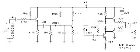
The TRF radio above operates on the AM broadcast band in the range of 550-1650 Khz.It's similar to a crystal radio with the addition of a couple buffer stages andaudio amp to drive a speaker. Reception is limited to strong local stations. KFI(Los Angeles) comes in loud and clear at a range of about 7 miles from the 50KWstation. KNX (1070) and KLAC (570) can be heard at low levels and a few otherstations can be barely heard if I put my ear against the speaker. The receiver usesa 16 inch square loop antenna wound on a wooden frame (13 turns #18) with a variable(30-365pF) capacitor. Larger loops would probably work better. Also, performancemight be better if the loop is rotated 45 degrees, so the frame looks like across (+) instead of an X. That way, the top and bottom sides will not be parallelto the ground, and the antenna will have more height.The antenna signal is buffered by the first emitter follower stage which presentsabout 150K input impedance. The buffer stage avoids losing much voltage from theantenna when connected to the circuit. The buffered RF voltage at the emitter ofthe transistor is rectified by the diode, and the RF component removed by thecapacitor at the base of the second transistor. This leaves only the audio signalat the base with about 5X higher amplitude at the collector. The 3 remainingtransistors form an audio amp to drive the 8 ohm speaker. The transistors usedare 2N3906 (PNP) and 2N4123 (NPN) however 2N3904 should work as well. The 100Kvariable resistor shown is only used to reduce the volume of very strong stations,such as KFI in my case. The speaker is a 4 inch model with a heavy 4 inch magnetinside a 6 inch box. Seems to be more efficient than speakers with smaller magnets.Headphones work better and I can hear 8 stations in the Los Angeles area at lowvolume. The complete circuit draws about 10mA from a 9 volt battery. (View)
View full Circuit Diagram | Comments | Reading(1961)
FM Beacon Broadcast Transmitter (88-108 MHz)
Published:2012/10/18 22:42:00 Author:muriel | Keyword: FM , Beacon Broadcast , Transmitter, 88-108 MHz
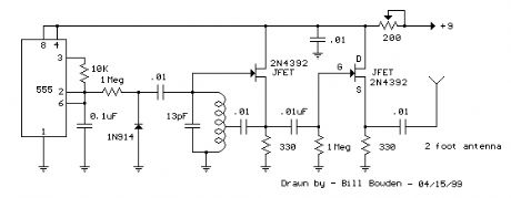
This circuit will transmit a continuous audio tone on the FM broadcast band (88-108 MHz) which could used for remote control or security purposes. Circuit draws about 30 mA from a 6-9 volt battery and can be received to about 100 yards. A 555 timer is used to produce the tone (about 600 Hz) which frequency modulates a Hartley oscillator. A second JFET transistor buffer stage is used to isolate the oscillator from the antenna so that the antenna position and length has less effect on the frequency. Fine frequency adjustment can be made by adjusting the 200 ohm resistor in series with the battery. Oscillator frequency is set by a 5 turn tapped inductor and 13 pF capacitor. The inductor was wound around a #8 X 32 bolt (about 3/16 diameter) and then removed by unscrewing the bolt. The inductor was then streached to about a 3/8 inch length and tapped near the center. The oscillator frequency should come out somewhere near the center of the band (98 MHz) and can be shifted higher or lower by slightly expanding or compressing the inductor. A small signal diode (1N914 or 1N4148) is used as a varactor diode so that the total capacity in parallel with the inductor varies slightly at the audio rate thus causing the oscillator frequency to change at the audio rate (600 Hz). The ramping waveform at pins 2 and 6 of the timer is applied to the reversed biased diode through a large (1 Meg) resistor so that the capacitance of the diode changes as the ramping voltage changes thus altering the frequency of the tank circuit. Alternately, an audio signal could be applied to the 1 Meg resistor to modulate the oscillator but it may require an additional pullup resistor to reverse bias the diode. The N channel JFET transistors used should be high frequency VHF or UHF types (Radio Shack #276-2062 MPF102) or similar. (View)
View full Circuit Diagram | Comments | Reading(1008)
Micro Power AM Broadcast Transmitter
Published:2012/10/18 22:40:00 Author:muriel | Keyword: Micro Power, AM , Broadcast Transmitter

In this circuit, a 74HC14 hex Schmitt trigger inverter is used as a square wave oscillator to drive a small signal transistor in a class C amplifier configuration. The oscillator frequency can be either fixed by a crystal or made adjustable (VFO) with a capacitor/resistor combination. A 100pF capacitor is used in place of the crystal for VFO operation. Amplitude modulation is accomplished with a second transistor that controls the DC voltage to the output stage. The modulator stage is biased so that half the supply voltage or 6 volts is applied to the output stage with no modulation. The output stage is tuned and matched to the antenna with a standard variable 30-365 pF capacitor. Approximately 20 milliamps of current will flow in the antenna lead (at frequencies near the top of the band) when the output stage is optimally tuned to the oscillator frequency. A small 'grain of wheat' lamp is used to indicate antenna current and optimum settings. The 140 uH inductor was made using a 2 inch length of 7/8 inch (OD) PVC pipe wound with 120 turns of #28 copper wire. Best performance is obtained near the high end of the broadcast band (1.6 MHz) since the antenna length is only a very small fraction of a wavelength. Input power to the amplifier is less than 100 milliwatts and antenna length is 3 meters or less which complies with FCC rules. Output power is somewhere in the 40 microwatt range and the signal can be heard approximately 80 feet. Radiated power output can be approximated by working out the antenna radiation resistance and multiplying by the antenna current squared. The radiation resistance for a dipole antenna less than 1/4 wavelength is
R = 80*[(pi)^2]*[(Length/wavelength)^2]*(a factor depending on the form of the current distribution) The factor depending on the current distribution turns out to be [(average current along the rod)/(feed current)]^2 for short rods, which is 1/4 for a linearly-tapered current distribution falling to zero at the ends. Even if the rods are capped with plates, this factor cannot be larger than 1. Substituting values for a 9.8 foot dipole at a frequency of 1.6 MHz we get R= 790*.000354*.25 = .07 Ohms. And the resistance will be only half as much for a monopole or 0.035 Ohms. Radiated power at 20 milliamps works out to about I^2 * R = 14 microwatts.
(View)
View full Circuit Diagram | Comments | Reading(2503)
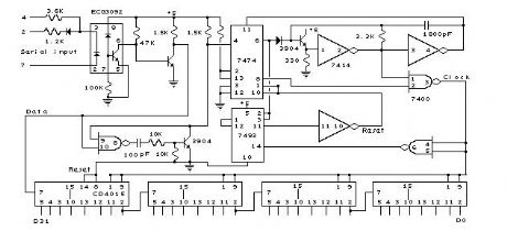
PC Serial Receiver (57.6K Baud / TTL & CMOS)
Published:2012/10/18 22:34:00 Author:muriel | Keyword: PC , Serial Receiver , 57.6K Baud , TTL & CMOS
View full Circuit Diagram | Comments | Reading(816)
PC Serial Port Receiver
Published:2012/10/18 22:33:00 Author:muriel | Keyword: PC , Serial Port , Receiver
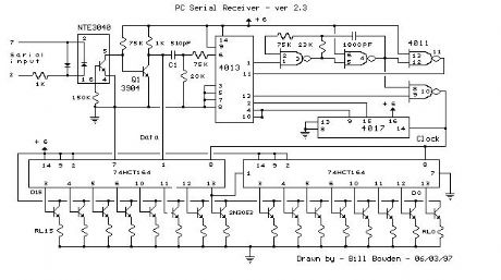
This circuit was designed to control a 32 channel Christmas light show from the PC serial port. Originally designed with TTL logic, it has been simplified using CMOS circuits to reduce component count. It is a fairly simple, reliable circuit that requires only 4 common CMOS chips (for 8 outputs), an optical isolator, and a few discrete components. The schematic diagram (SERIAL.GIF) illustrates the circuit with 16 outputs which can be expanded with additional 8 bit shift registers. (View)
View full Circuit Diagram | Comments | Reading(1177)
Commonly used simple oscillator circuit diagram
Published:2012/10/17 22:16:00 Author:Ecco | Keyword: oscillator
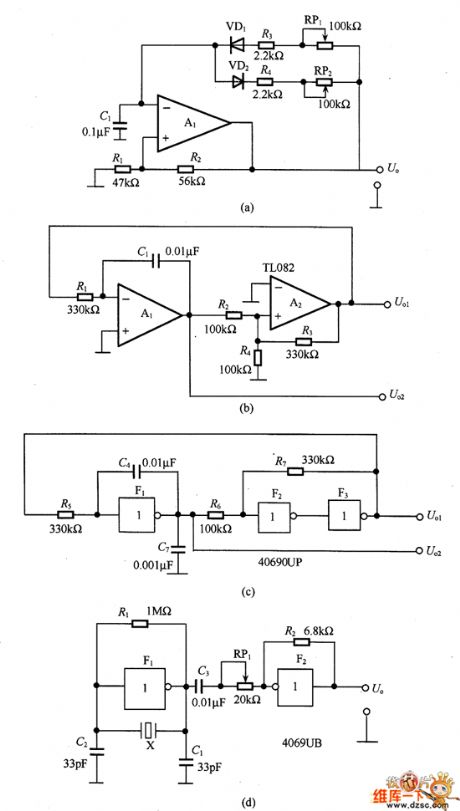
Figure (a) is the square wave output circuit, in the circuit, the op amp A1 is added a positive feedback, i.e., feedback resistor R2 is connected between the noninverting input and output terminals to form a comparator circuit with the delay characteristics. The voltage on R1 and the charging and discharging voltageof capacitor C1 cause oscillation from comparison. High and low level time of output square wave can be set independently, and the oscillation frequency is determined by the high and low level time, namely, it uses diodes VD1 and VD2, potentiometer RP1 and RP2 to set the charging and discharging time of capacitor C1.
(View)
View full Circuit Diagram | Comments | Reading(1425)
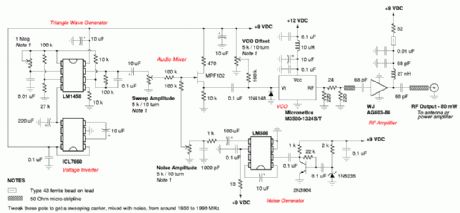
Linear voltage-controlled oscillator circuit diagram
Published:2012/10/17 22:05:00 Author:Ecco | Keyword: Linear, voltage-controlled oscillator
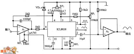
It uses ICL8038 to form a linear voltage controlled oscillator with output frequency and input voltage being proportional. In the circuit, A1 is used to improve C1 charging and discharging constant current circuit characteristics, so that the output frequency and relative input voltage have a linear relationship, A2 is the sine wave output buffer. RP1 is used to adjust the offset voltage, RP2 is used to adjust the high-frequency symmetry, RP3 is used to adjust the low-frequency symmetry, RP3 and RP4 are used to adjust the sine-wave distortion degree.
(View)
View full Circuit Diagram | Comments | Reading(2420)
Voltage - controlled oscillator circuit diagram with operational amplifier
Published:2012/10/17 23:03:00 Author:Ecco | Keyword: Voltage - controlled oscillator , operational amplifier
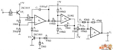
The circuit uses integrator A1 and delay comparator A2 to form a triangular wave oscillator, but the circuit is not directly integrating the output of A2, but it's controlled for integrating, therefore, the obtained oscillation frequency and control voltage are proportional, i.e. the so-called voltage-controlled oscillator. In the circuit, when VT2 gets conduction, the discharging slope rate of C1 is contrary to charging to generate a triangular wave. Saturation voltage of the op amp A2 affects Delay comparator threshold. Thus, the circuit is not suitable for high accuracy circuit. A3 is level-shifting circuit.
(View)
View full Circuit Diagram | Comments | Reading(2957)
Infrared headphones transmitter circuit
Published:2012/10/11 21:17:00 Author:muriel | Keyword: Infrared, headphones, transmitter
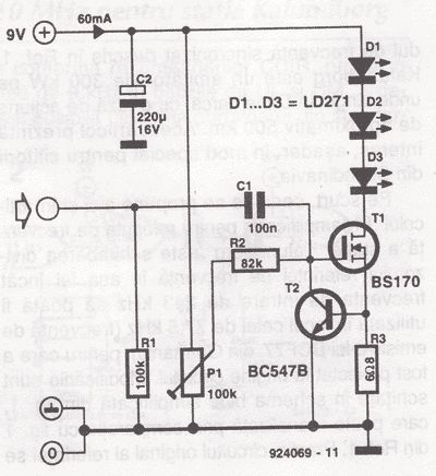
The transmitter offers a optical link (infrared) for headphones. Three infrared leds (ir) are polirised by T1 current, P1 is used to adjust the current level . Current consumption of this headphones infrared transmitter is about 60mA at 9V.Maintain separated adapter ground and audio signal ground to prevent current reactions thru LED. The optical link is relative directional and can be improved by placing the leds in different angles and placing reflectors behind them.
The optimal input audio level is 100 – 200mV for 1.2 – 2.4 m coverage of this headphones ir transmitter.On the site we provide the infrared receiver schematic for this infrared headphones transmitter.
Infrared headphones transmitter circuit
(View)
View full Circuit Diagram | Comments | Reading(1878)
Infrared headphones receiver circuit
Published:2012/10/11 21:17:00 Author:muriel | Keyword: Infrared, headphones, receiver
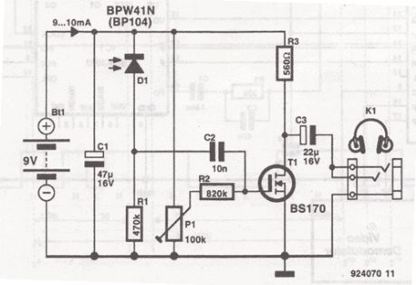
Use this infrared headphones receiver with the ir headphones transmitter.Use 600Ω headphones. BPW41N and BP104 have a filter for visible light and are centered on 950nm at 250C.At normal light illumination and 3 to 4 meters distance the audio distorsion were 1 – 2%, wich is not bad for such a simple ir headphones receiver schematic
IR headphone receiver circuit diagram
(View)
View full Circuit Diagram | Comments | Reading(1383)
Booster for Cable Radio
Published:2012/10/11 21:09:00 Author:muriel | Keyword: Booster, Cable Radio
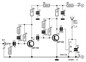
With the aid of this circuit it is possible to listen, using a portable VHF FM radio, to listen to stations that transmit only your local cable network. Both from its properties and its design this ‘cable booster’ appears similar to an antenna amplifier, because this is a two-stage amplifier with two common RF transistors type BF199.Only this time, the input is connected to the cable connection instead of an antenna while the output does not contain a coaxial connection but a tuned circuit that acts as impedance matching for a 1/4λ-antenna. If the circuit is tuned correctly (using trimmer C8), the amplified cable signal is radiated by the vertical antenna and can be easily received by a portable receiver up to three metres away.
Cable radio booster circuit diagram
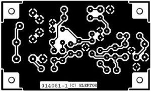
It is always possible to build the circuit on a piece of prototyping board, but because an RF-circuit is usually a little more critical it will probably work a lot better if you make use of the PCB layout shown here. During the design, the essential connections have been kept short and the ground plane has been made as large as possible. Capacitor C7 is best directly connected to the tap on L1, as can be seen in the photo. The (air-cored) coil consists of three turns of 1-mm enamelled copper wire (ECW) wound around a pencil (diameter about 8 mm).
Cable radio amplifier PCB layout
(View)
View full Circuit Diagram | Comments | Reading(1425)
Frequency Modulated Oscillator
Published:2012/10/11 21:09:00 Author:muriel | Keyword: Frequency, Modulated Oscillator
This FM oscillator can be used for wireless audio, microphone and part-15 applications where stable frequency modulated oscillators is needed. Lt can be varied to cover 75 to 150 MHz, as needed.
FM oscillator circuit schematic
(View)
View full Circuit Diagram | Comments | Reading(1837)
VLF VHF wideband active antenna
Published:2012/10/11 21:08:00 Author:muriel | Keyword: VLF, VHF, wideband, active antenna
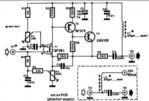
A 30 to 50 cm whip antenna provides reception from 10 MHz to over 220 MHz. T1 BF981, a dual-gate MOSFET, provides low noise, high-input impedance and high gain. The circuit is powered via the coaxial cable used to connect the antenna to a receiver.
Wideband active antenna amplifier circuit
(View)
View full Circuit Diagram | Comments | Reading(2464)
Stereo TV decoder
Published:2012/10/11 2:36:00 Author:muriel | Keyword: Stereo TV, decoder
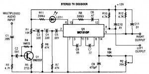
A simple stereo tv decoder circuit build with MC1310P. Transistor Q1 is an audio amplifier and U1 is used as a 31.5KHz subcarrier which is similar to 38KHz FM MPX. Pilot frequency is 15.734KHz.
Stereo tv decoder schematic
(View)
View full Circuit Diagram | Comments | Reading(4435)
27MHz NBFM Transmitter
Published:2012/10/11 2:36:00 Author:muriel | Keyword: 27MHz, NBFM Transmitter
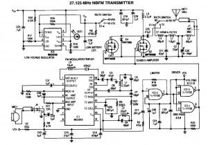
A 27MHz NBFM transmitter circuit schematic with MC2833 and 2 FET transistors MPF6660. Using a Motorola MC2833 one-chip FM transmitter, a few support components and am MPF6660 RF amp, this transmitter delivers up to 3W into a 50 Ω antenna. It is capable of operation over about 29 to 32 MHz with the components shown.
27MHz NBFM transmitter circuit diagram
(View)
View full Circuit Diagram | Comments | Reading(2861)
Signal meter circuit
Published:2012/10/11 2:32:00 Author:muriel | Keyword: Signal meter
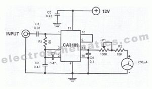
The CA3189 IC integrates a symmetrical limiter, a phase demodulator, an audio amplifier, and a logarithmic detector-amplifier. The logarithmic detector-amplifier is the most interesting part of the IC for the above featured circuit. It can be used to enhance the “logarithmic signal meter” of shortwave receivers to make the signal reading more accurate.Building the circuit is very simple. It must be built in such a way that it will work up to 30 MHz. To do that, follow these guidelines: connect the input to a 50 Ω line; make the circuit wiring as short as possible; and the input signal must be shielded.
Signal meter circuit schematic
(View)
View full Circuit Diagram | Comments | Reading(1423)
Cell phone jammer circuit
Published:2012/10/11 2:30:00 Author:muriel | Keyword: Cell phone, jammer
A beautiful diy gsm jammer or mobile cell phone jammer schematic diagram for use only in GSM1900 with frequency from 1930 MHz to 1990 MHz. The GSM1900 mobile phone network is used by USA, Canada and most of the countries in South America.
Mobile cellphone jammer circuit diagram
This cell phone jammer is not applicable for use in Europe, Middle East, nor Asia.The GSM jammer circuit could block mobile phone signals which works on GSM1900 band, also called DCS. For more cell phone jammers check the related posts.
(View)
View full Circuit Diagram | Comments | Reading(2498)
Spy phone transmitter
Published:2012/10/11 2:30:00 Author:muriel | Keyword: Spy phone, transmitter
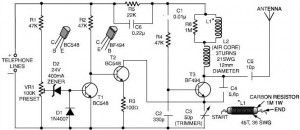
Here is a very simple telephone broadcaster or transmitter which can be used to eavesdrop on a telephone conversation. The circuit can also be used as a wireless telephone amplifier.One important feature of this phone transmitter is that the circuit derives its power directly from the active telephone lines, and thus avoids use of any external battery or other power supplies.This not only saves a lot of space but also money. It consumes very low current from telephone lines without disturbing its performance. The phone bug transmitter is very tiny and can be built using a single -IC type veroboard that can be easily fitted inside a telephone connectin box of 3.75cm x 5cm.
The spy phone transmitter consists of two sections, namely, automatic switching section and FM transmitter section.
Spy phone transmitter circuit diagram
Automatic switching section comprises resistors R1 to R3, preset VR1, transistor T1 and T2, zener D2 and diode D1. Resistor R1, along with preset VR1, works as a voltage divider. When voltage across the telephone lines is 48V DC, the voltage available at wiper of preset VR1 ranges from 0 to 32V (adjustable).
The switching voltage of the circuit depends on zener breakdown voltage and switching voltage of the transistor T1. Thus, if we adjust preset VR1 to get over 24.7 volts, it will cause the zener to breakdown and transistor T1 to conduc. As a result collector of transistor T1 will get pulled towards negative supply, to cut off transistor T2. At this stage, if you lift the handset of the telephone, the line voltage drops to about 11V and transistor T1 is cut off. As a result, T2 gets forward biased through R2 to provide a DC path for T3 used in the following FM transmitter section.
The low-power FM transmitter section comprises oscillator transistor T3, coil L1 and a few other components. T3 works as a common-emitter RF oscillator, with T2 serving as an electronic “on/off” switch. The audio signal available across the telephone lines automatically modulates oscillator frequency via T2 along with its biasing R3. The modulated RF signal is fed to the antenna. The telephne conversation can be heard on an FM receiver remotely when it is tuned to the transmitter frequency.
(View)
View full Circuit Diagram | Comments | Reading(1394)
Quality FM transmitter circuit
Published:2012/10/11 2:28:00 Author:muriel | Keyword: Quality, FM transmitter
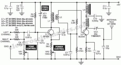
This house FM transmitter for your stereo or any other amplifier provides a good signal strength up to a distance of 500 meters with a power output of about 200 mW. It works off a 9V battery.
The audio-frequency modulation stage is built around transistor BF494 (T1), which is wired as a VHF oscillator and modulates the audio signal present at the base. Using preset VR1, you can adjust the audio signal level.Audio FM transmitter circuit diagram
The VHF frequency is decided by coil L1 and variable capacitor VC1. Reduce the value of VR2 to have a greater power output.The next stage is built around transistor BC548 (T2), which serves as a Class-A power amplifier. This stage is inductively coupled to the audio-frequency modulation stage. The antenna matching network consists of variable capacitor VC2 and capacitor C9. Adjust VC2 for the maximum transmission of power or signal strength at the receiver.
If you design a good pcb layout you can use it as a car fm transmitter.For frequency stability, use a regulated DC power supply and house the transmitter inside a metallic cabinet. For higher antenna gain, use a telescopic antenna in place of the simple wire. Coils L1 and L2 are to be wound over the same air core such that windings for coil L2 start from the end point for coil L1. Coil windingdetails are given below:L1: 5 turns of 24 SWG wire closely wound over a 5mm dia. air coreL2: 2 turns of 24 SWG wire closely wound over the 5mm dia. air coreL3: 7 turns of 24 SWG wire closely wound over a 4mm dia. air coreL4: 5 turns of 28 SWG wire on an intermediate-frequency transmitter (IFT) ferrite coreCheck the related posts for some stereo fm transmitter circuits.
(View)
View full Circuit Diagram | Comments | Reading(2268)
| Pages:35/195 At 202122232425262728293031323334353637383940Under 20 |
Circuit Categories
power supply circuit
Amplifier Circuit
Basic Circuit
LED and Light Circuit
Sensor Circuit
Signal Processing
Electrical Equipment Circuit
Control Circuit
Remote Control Circuit
A/D-D/A Converter Circuit
Audio Circuit
Measuring and Test Circuit
Communication Circuit
Computer-Related Circuit
555 Circuit
Automotive Circuit
Repairing Circuit