
Basic Circuit
Index 428
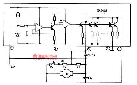
KA2402-motor speed-stable integrated circuit diagram
Published:2011/5/5 1:44:00 Author:Nicole | Keyword: motor speed-stable
KA2402 is a DC motor speed-stable integrated circuit which is produced by South Korea's Samung, it is widely used in all kinds of super miniature, miniature audio, it is as motor drive circuit.
1, KA2402 internal circuit and pin function
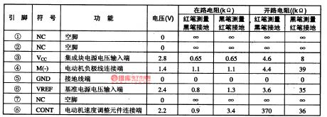
KA2402 integrated block internal circuit and typical application circuit is shown in the figure 1-1. This IC has two kinds of package type, KA2402 is 8-foot dual in-line structure, KA2402 is 8-foot dual line flat type structure. The pin function and data of this integrated circuit is shown in the chart 1-1. The former voltage range is Vcc=1.8-8V, the later is 1.8-5V.
Figure 1-1 KA2402 integrated block internal circuit and typical application circuit is shown.
2, KA2402 typical application circuit
KA2402 integrated block typical application circuit is shown in the figure 1-1. (View)
View full Circuit Diagram | Comments | Reading(1825)
The typical application circuit diagram of LA1185 IC
Published:2011/5/5 1:28:00 Author:Ecco | Keyword: typical application circuit, IC
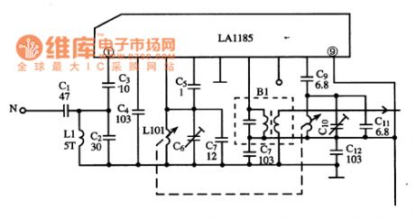
The typical application circuit diagram of LA1185 IC is shown as the chart.
Tip: FM radio signal passes band-pass filter composed of C1, L1, C2, and the signal without FM band is filtered and then coupled by C3, then it is added LA1185 ① feet, it is amplified and added to the mixer oscillator circuit, and it will be made vibration signal mix with the local signal sent by the local oscillator circuit, the resulting difference frequency signal is output from ⑥ feet, and the filter composed of B1 will select 10.7MHz IF signal and send it to later level circuit to do further treatment.
(View)
View full Circuit Diagram | Comments | Reading(4631)
STV2180 Color baseband delay line integrated circuit diagram
Published:2011/5/5 1:44:00 Author:Ecco | Keyword: Color baseband , delay line , integrated circuit
STV2180 is the color baseband delay line integrated circuit produced by SGS-THOMSON company in French, it is widely used in various domestic and imported color television sets, such as TCL, High Road, Hua, Skyworth, Hisense and other products. 1. Features of function STV2180 integrated circuit is mainly composed of (R-Y) and (B-Y) signal processing circuit, sand castle pulse signal processing circuit, the delay processing circuit, the buffer signal processing circuit, and other ancillary functions circuit. 2. Pin functions and data STV2180 IC uses 14-pin dual in-line plastic package, the pin functions and data are listed in Table. STV2180 IC pin functions and data
(View)
View full Circuit Diagram | Comments | Reading(588)
STV2116 color decoding and scanning signal processing integrated circuit diagram
Published:2011/5/5 1:57:00 Author:Ecco | Keyword: Color , decoding , scanning , signal , processing, integrated circuit
STV2116 is the color decoding and scanning signal processing integrated circuit produced by SGS-THOMSON company in French, it is widely used in various domestic and imported large screen color television sets, such as Skyworth, TCL and so on. 1. Features of functionSTV2116 IC is mainly composed of the clock oscillator circuit, automatic color elimination control circuit, data and clock interface circuit, the volume control circuit, the character BRG signal processing circuit, ribbon pass and notch adjustment circuit, the character blanking signal processing circuit, the luminance signal or video signal processing circuit, color signal processing circuit, small-field scanning line signal processing circuit and other ancillary functions circuit. 2. Pin functions and data STV2116 IC uses million inline package with 42 feet in double rows, the pin functions and data are listed in Table. STV2116 IC pin functions and data
(View)
View full Circuit Diagram | Comments | Reading(822)
Two LEDs alternately flashing circuit diagram controlled by digital integrated circuit
Published:2011/5/5 2:28:00 Author:Ecco | Keyword: Two, LED alternately, flashing , controlled , digital integrated circuit
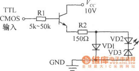
The circuit shown as the chart is controlled by TTL or CMOS digital integrated circuit, it will flash alternately by the transistor conduction to drive two LED lights. Different supply voltage can change the R and the regulation value of VD3 to meet the requirements of two alternately flashing. (View)
View full Circuit Diagram | Comments | Reading(587)
Power supply working status indication circuit
Published:2011/5/5 2:22:00 Author:Ecco | Keyword: Power supply , working status , indication circuit
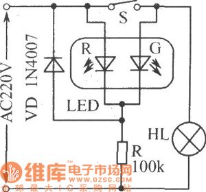
In the circuit shown as the chart, LED-R is used as a power indicator, LED-G is load HL (light) work status indicator. When the 220V AC electric supply is normal, LED-R emits red light. When switch S is closed, HL is lit, LED-G emits green light, then LED-R is also the lit, so when S is closed, the two-tone LED emits orange color.
(View)
View full Circuit Diagram | Comments | Reading(1441)
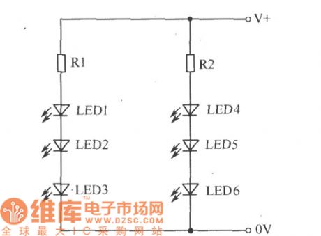
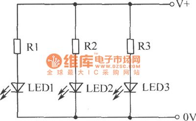
The driver circuit diagram with many LEDs
Published:2011/5/5 2:12:00 Author:Ecco | Keyword: driver circuit, many, LED
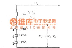
The LED connected in series can be driven by a current-limiting resistor:
The circuit can drive any number of LEDs:
The circuit uses the parallel method to drive a lot of LEDs:
(View)
View full Circuit Diagram | Comments | Reading(685)
Platinum resistance signal conditioner ADT70 interior circuit diagram and typical application circuit diagram
Published:2011/4/21 21:40:00 Author:muriel | Keyword: Platinum resistance signal conditioner
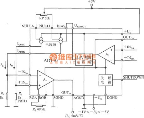
As shown is Internal circuit diagram and typical application circuit of platinum resistance signal conditioner ADT70. There are five parts of the chip:1. 2.5V reference voltage source2. two balanced output type current source3. instrument amplifier A14. reserve amplifier A25. turn-off circuit
In the picutre it uses the double-power supply. When -Us is at least -1V, it can measure the temperature below 0°C. The SGND、AGND and DGNA are all grounding. When SHUTDOWN non-connected the DGND, the ADT70 is turned-off; Without the end, it should be connected the +Us. When +5V power supply go through the potentiometer, it will supply the current source power. The 2.5V reference voltage sourceprovides bias to the current source. Two current source respectiveprovide exciting current for nominal resistance R1 and platinum resistance R2, The voltage difference of R2 and R1 is used for the input voltage of instrument amplifier. After adjust the gain of the instrument amplifier, It can obtain the output voltage Uo which vary directly as the measured temperature, final it send to the digital voltmeter that will show the measured temperature value. The resistence of R1 is 1KΩ. R2 is Pt1000 platinum resistance, its nominal resistence is 1kΩ below 0°C. RP is tone balance potentiometer. R3 is gain resistance of instrument amplifier.
(View)
View full Circuit Diagram | Comments | Reading(1078)
The typical application circuit diagram of LA1260 IC
Published:2011/5/5 1:14:00 Author:Ecco | Keyword: typical application circuit , IC
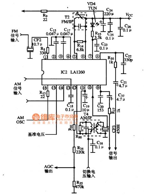
The typical application circuit
The typical application circuit of radio composed of LA1260 IC is shown as the chart. Tip: the pin of LAl260 IC is the input end of AM / FM band switching control signal, when the pin is floating, LAl260 is in the FM working state, when the feet connects to the power supply, it is in the AM state. AM / FM switch exception should check the pin voltage firstly.
The typical application circuit diagram of LA1260 IC is shown as the chart. (View)
View full Circuit Diagram | Comments | Reading(4468)
The typical application circuit diagram of LA4140 IC
Published:2011/5/5 1:08:00 Author:Ecco | Keyword: typical application circuit, IC
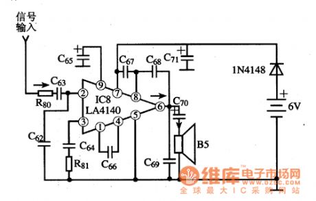
The typical application circuit
The typical application circuit of audio amplifier circuit composed of LA4140 IC is shown in Figure below.
The typical application circuit diagram of LA4140 IC is shown as the chart. (View)
View full Circuit Diagram | Comments | Reading(3762)
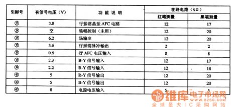
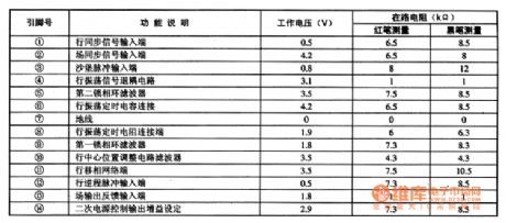
TEA5114A-RGB switch integrated circuit diagram
Published:2011/5/5 1:03:00 Author:Ecco | Keyword: RGB , switch, integrated circuit
TEA5114A is the RGB switch integrated circuit produced by Thomson company in French, it is widely used in series brands of color TV and color monitors, such as Changhong series of rear projection color TV sets. 1. Features of functionTEA5114A integrated circuit is mainly composed of the RGB color signal processing circuit and associated switching circuit. 2. Pin functions and data TEA5114A IC uses 16-pin dual in-line package, the pin functions and data are listed in Table 1. Table 1 shows TEA5114A pin function and data.
(View)
View full Circuit Diagram | Comments | Reading(673)
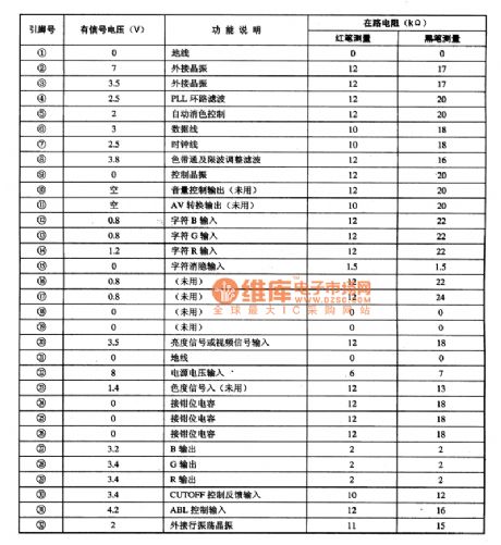
TDA9187 picture quality improvement IC diagram
Published:2011/5/4 22:43:00 Author:Ecco | Keyword: picture quality, improvement, IC
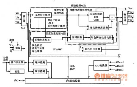
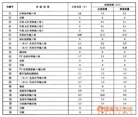
TDA9187 is picture quality improvement IC produced by Philips, it is widely used in Changhong projection color TV series. 1. Features of functionTDA9187 integrated circuit includes pulse signal processing circuit, color saturation correction circuit, the luminance signal processing circuit, the definition improvement circuit, colour transient improvement circuit, the delay control circuit, color signal processing circuit, A / D converter, I2C bus control circuit. The block diagram of the circuit is shown in Figure 1. Figure 1 shows the block diagram of TDA9187 integrated circuit.
2. Pin functions and data TDA9187 integrated circuit uses 24-pin dual in-line package, the pin functions and data are listed in Table 1. Table 1 shows TDA9187 integrated circuit pin functions and data.
(View)
View full Circuit Diagram | Comments | Reading(643)
TDA9112-I2C bus control row / field scanning integrated circuit diagram
Published:2011/5/4 21:53:00 Author:Ecco | Keyword: bus control, row , field , scanning , integrated circuit
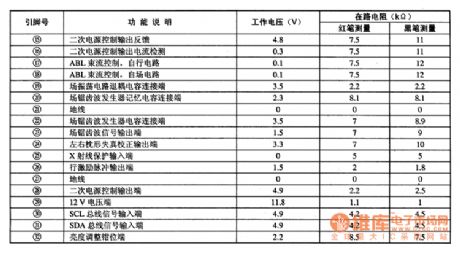
TDA9112 is the bus control row / field scanning integrated circuit produced by Philips, it is widely used in color displays, such as Tsinghua Tongfang series of color display. 1. Features of functionTDA9112 IC includes I2C bus interface circuit, the line oscillator circuit, field oscillation and the sawtooth wave generating circuit, left and right pincushion correction circuit, the line excitation circuit, PLL circuit, the same frequency signal processing circuit, ABL beam current system circuit, X-ray protection circuit, and other auxiliary functions circuit. 2. Pin functions and dataTDA9112 IC uses 32-pin dual in-line package, the pin functions and the number are shown in Table 1. Table 1 shows TDA9112 integrated circuit pin functions and data.
(View)
View full Circuit Diagram | Comments | Reading(558)
Capacitor fourth-order low-pass filter circuit diagram
Published:2011/5/4 22:42:00 Author:Rebekka | Keyword: Fourth-order low-pass capacitor filter
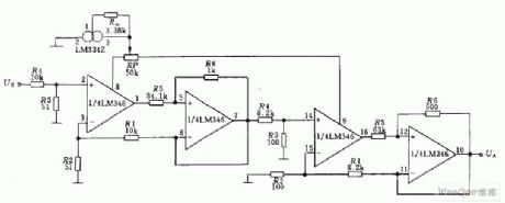
Capacitor fourth-order low-pass filter circuit is shown as below. The circuit uses an LM348 op amp four high-level low-pass filter circuit. For example, fc = 20KHz, filter transmission coefficient is Ho = 1, Q01 = 0.514, Q02 = 1.306. Because the count of band-pass amplification factor is the same with the four amplifiers. So it is enough to equip with a current source (LM334Z). You can have a precise adjustment by potentiometer RP. (View)
View full Circuit Diagram | Comments | Reading(2090)
TB31224 communication RF complex integrated circuit
Published:2011/5/4 10:03:00 Author:TaoXi | Keyword: communication, RF, complex
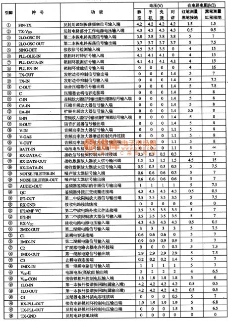
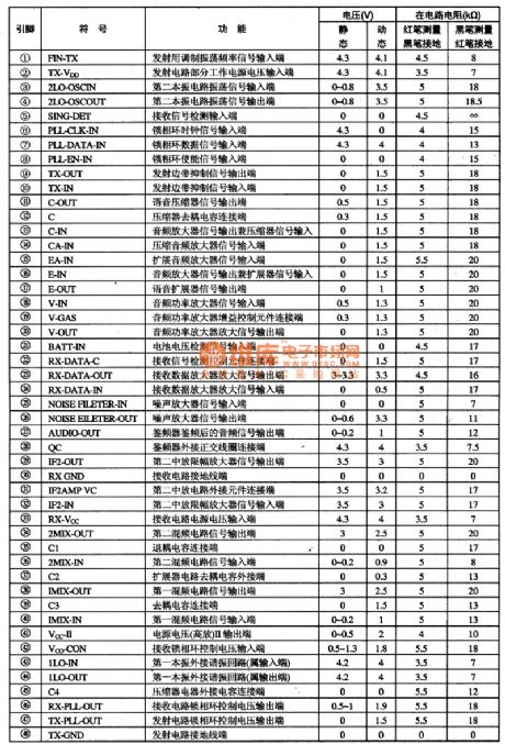
The TB31224 is the communication RF complex integrated circuit that can be used in various models of cordless telephone.
1.Features
The TB31224 is composed of the transmit and receive signal processing circuit, the phase-locked loop signal processing circuit, the audio compression and expansion circuit, the double-conversion processing circuit.etc. This circuit can completes the receive demodulation, PLL control and language processing & compression & extension functions.
2.Pin functions and data
The TB31224 is in the 48-pin package, and the pin functions and data of the host RF complex integrated circuit TB31224 is as shown in table 1. The mobile phone RF integrated circuit TB31224's pin functions and data is as shown in table 2.
Tips: TC31224's pin functions and data is the same as the TB31224's, they are the interchangeable devices.
Table 1 pin functions and data of the host RF complex integrated circuitTB31224
Table 2 The pin functions and data of thecellphoneRF complex integrated circuitTB31224 (View)
View full Circuit Diagram | Comments | Reading(1083)
Pincushion Correction Circuit-Discrete Circuit Diagram
Published:2011/5/4 8:17:00 Author:Robert | Keyword: Pincushion Correction, Discrete
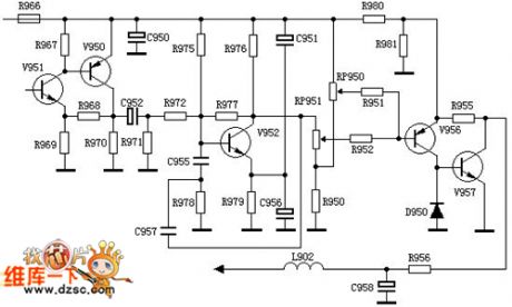
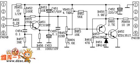
It is the parabolic wave signal addedon the r520, and the user can adjust the parabolic wave signal amplitude by adjusting the r520, which canadjust the pincushion correction value as well. It is DC voltage added on the r523, and the user can adjust the line width by adjusting r523.
This second circuit extracted from the Venus d2918 type pincushion correction circuit, whichhasjust V951 and v950 two-stage amplification more than the firstpincushion correction circuit shown below. The reason is that the field sawtooth wave is not taken from field deflection coilssampling resistor, but from tda8838's 46 foot, so thatit'sadded a two-stage amplification due to its small magnitude.
The models which use this pincushion correction circuit have: Korea Samsung mc-15 module, Venus c6418, v6458, Peony 64c1, Lehua ct6388w and so on.
The field sawtooth wave voltage is send to the pincushion correction circuit from the p404's 4 foot, and the r455, c454, r457 make up the integral circuit to integrate the field swatooth wave and produce the up-convexparabolic wave voltage. This voltage then is added on the b polar of the parabolic wave shaping and amplifying tube. Afteramplifying and shaping the c polar output 9V (peak-peak value) down-convex parabolic wave voltage. Then after the level width adjustment, left-rightpincushion distortion adjustment network made up by the vr451, vr452, r464, r463, r462, this voltage wave is added to the polar of the compound tube made up by q453 and q452. After amplifying the q452's c polar outputs 12.5V (peak-peak value) parabolic wave voltage. At last this voltage wave is send to the line scan circuit from fr459 and p403's 3 foot to modulate the line scan current. So this process achieve the goal of pincushion distortioncorrection.
The vr451 is theline width adjustment potentiometer, thevr452 is pincushion distortion correction potentiometer.
(View)
View full Circuit Diagram | Comments | Reading(1653)
Parallel Capacitor Circuit
Published:2011/5/4 8:19:00 Author:Robert | Keyword: Parallel, Capacitor

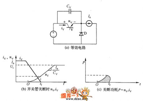
1.Parallel Capacitor
The simplestturn-off snubber circuitis to add the switch with a parallel capasitor Cv, which is shown in picture 1 (a), to limit the rising speed of the switch tubevoltage during its closing time which is shown below. The current before the switch tubeclosed is Io. The more Cv is, the slower therising speed of the switch tube voltageis, and the less power consumption of switch would be. The picture 1(b) and (c) shows the Uv, Iv and P during the closing time in separately. The picture 1 shows the parallel capacitor of the switch tube in the buck converter.
(View)
View full Circuit Diagram | Comments | Reading(718)
TSV type temperature sensor measurement diagram using constant current
Published:2011/5/4 7:47:00 Author: | Keyword: temperature sensor, constant current
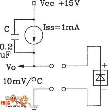
In a TSV type temperature sensor measurement diagram using constant current, when using constant current as load , the load current will not change,voltage drop of lead wire is a constant,so the ouput voltage will change according to10mV/℃.Usually control distant can reach up to thousand meters.
(View)
View full Circuit Diagram | Comments | Reading(493)
two-channel high-speed high-gain optocoupler circuit diagram
Published:2011/5/4 9:28:00 Author:Nancy | Keyword: two-channel, high-speed, high-gain, optocoupler

View full Circuit Diagram | Comments | Reading(679)
crystal diode 3R3TI30E-080 internal circuit diagram
Published:2011/5/4 9:37:00 Author:Nancy | Keyword: crystal diode
View full Circuit Diagram | Comments | Reading(454)
| Pages:428/471 At 20421422423424425426427428429430431432433434435436437438439440Under 20 |
Circuit Categories
power supply circuit
Amplifier Circuit
Basic Circuit
LED and Light Circuit
Sensor Circuit
Signal Processing
Electrical Equipment Circuit
Control Circuit
Remote Control Circuit
A/D-D/A Converter Circuit
Audio Circuit
Measuring and Test Circuit
Communication Circuit
Computer-Related Circuit
555 Circuit
Automotive Circuit
Repairing Circuit