
Basic Circuit
Index 436
Five-function electronic watch circuit
Published:2011/4/26 0:55:00 Author:Nicole | Keyword: electronic watch
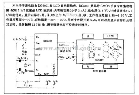
This electronic watch circuit is composed of DG5001 and LCD display. DG5001 is single chip CMOS watch special IC, it is adapted to 3 1/2 bit LCD, it has the advantage of micropower (lower than 3μA), low voltage(1.5V), small timing error(0.5s/d). The show contents: month, day, hour(morning A/afternoon P), minute, second. The range of work voltage is 1.35~3.50V, the range of temperature is 0~70℃, storage temperature is -20~+75℃. Using two perpheral switches S1, S2 can change the show contents and check of the timing. The crystals oscillation frequency is 32768Hz, adjusting the Trimmer capacitor can check of the time precision. (View)
View full Circuit Diagram | Comments | Reading(902)
Night vision benchmark circuit
Published:2011/4/26 0:35:00 Author:Nicole | Keyword: night vision, benchmark
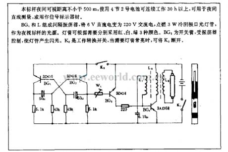
The night visual range of this benchmark is not shorter than 500m, using 4 2-type batteries, it can constantly work more than 30h, it can be used for night linear measuring, or used as singal device labelled.
Interval oscillator is composed of BG4 and L, it changes 6V DC power into 220V AC power, igniting 3W cold cathode fluorescent tube then to used it as the source of night vision benchmark. The tube can choose red, white, green three colors according to the needs. BG3 is switching tube, it is controlled by oscillator, to make tube flash. K2 is working transfer switch, when it is need to keep tube lighting, it can cut off K2. (View)
View full Circuit Diagram | Comments | Reading(1941)
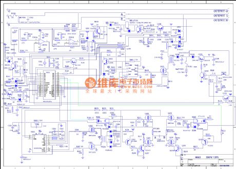
UPS circuit diagram
Published:2011/4/25 2:48:00 Author:May | Keyword: UPS
View full Circuit Diagram | Comments | Reading(7760)
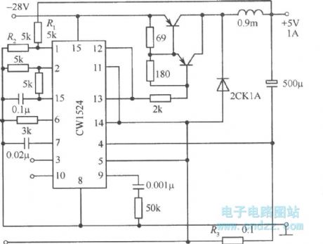
4V DC convertor connected by CWI524A
Published:2011/4/22 6:51:00 Author:May | Keyword: 4V, DC, convertor
View full Circuit Diagram | Comments | Reading(460)
Single end fly back type power converter circuit with energy returning winding diode clampling circuit
Published:2011/4/21 1:22:00 Author:May | Keyword: Single end, fly back, power converter, energy returning winding, diode clampling
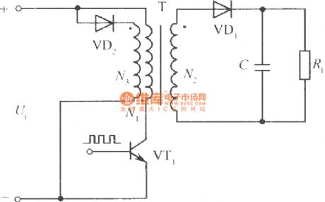
The following diagram is single end fly back type power converter circuit with energy returning winding diode clamping circuit. The turn number of N3 winding is equal to N1's, and the polarity of them is opposite. When VT1 is cutting off and the potential of collector increasing two times of input voltage, diode VD2 is breaking over, VT1's collector potential is clamped, leakage inductance stored energy is retuning to network.
In order to get relatively good effects, N2 and N1 must close coupling, and clamping diode VD2 can break over fast.
(View)
View full Circuit Diagram | Comments | Reading(593)
The inside circuit diagram of TIP131 and TIP132 crystal triode
Published:2011/3/24 3:34:00 Author:Ecco | Keyword: crystal triode
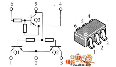
The inside circuit diagram of TIP131 and TIP132 crystal triode is as below:
(View)
View full Circuit Diagram | Comments | Reading(669)
The circuit diagram of frequency modulation receive in 50 KHz
Published:2011/3/24 3:28:00 Author:Ecco | Keyword: frequency modulation receive in 50 KHz
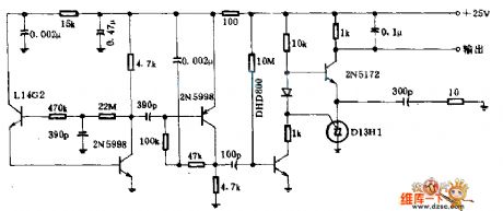
This circuitry is applied in pulse speed control system. In this system, the rate of pulse speed of modulating beam of light in the fiberis changed by the transimitter, and the rate of pulse speed is changed up and down in the center of 50KHZ frequency. The L14 G2 optics transistor changes the modulating light as semaphore of radio frequency for demodulation, and it can restore originally semaphore of radio frequency. (View)
View full Circuit Diagram | Comments | Reading(676)
Circuit Diagram of Third-order Asymmetric Filter
Published:2011/4/21 1:26:00 Author:Tina | Keyword: Third-order, Asymmetric
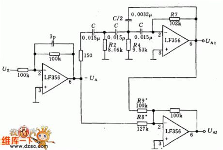
The Third-order Asymmetric Filter has two output channels (UA1 and UA2), UA1 is the high-pass filtered output channel and the UA2 is the low-pass filtered output channel. The circuit is as shown:
(View)
View full Circuit Diagram | Comments | Reading(570)
Flashing circuit with astable trigger
Published:2011/4/25 0:43:00 Author:Nicole | Keyword: flashing, astable trigger
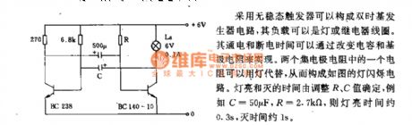
Double time base generator circuit can be composed of astable trigger, the load can be light or relay coil. The on/off time depend on the capacitance and base resistance. One of two collector resistances can be replaced by light, then to form the light flashing circuit. The time of light on/ off is decided by R, C, such as C=50μF, R=2.7KΩ, then the light time is about 0.3s, the off time is about 1s. (View)
View full Circuit Diagram | Comments | Reading(591)
TCM5089 microcomputer dial integrated circuit
Published:2011/4/24 22:51:00 Author:TaoXi | Keyword: microcomputer, dial integrated
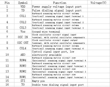
The TCM5089 microcomputer dial integrated circuit can be used in communication equipment as the pulse / tone signal generator.
1.Features
The TCM5089 IC has the pulse / tone dial compatible circuit, key switch signal encode and decode circuit.
2.Pin functions and data
The pin functions and data of the TCM5089 IC is as shown in table 1.
Table 1. The pin functions and data of the TCM5089 IC (View)
View full Circuit Diagram | Comments | Reading(770)
TCM5087 microcomputer dial integrated circuit
Published:2011/4/25 3:24:00 Author:TaoXi | Keyword: microcomputer, dial integrated
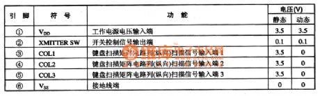
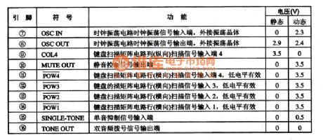
The TCM5087 microcomputer dial integrated circuit can be used in communication equipment as the Dual audio signal code generator.
1.Features
The TCM5087 IC has the dial-up signal encode circuit, key switch signal translate and edit circuit, and the mute control circuit.
2.Pin functions and data
The pin functions and data of the TCM5087 IC is as shown in table 1.
(View)
View full Circuit Diagram | Comments | Reading(635)
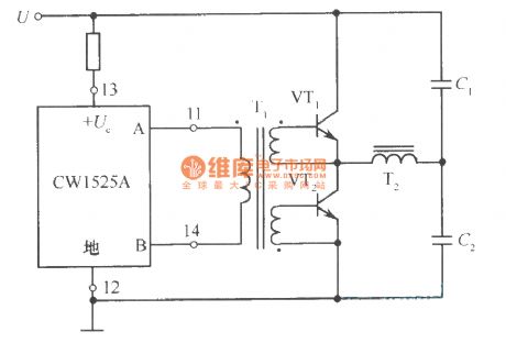
CWl525A driving M0S tube push-pull driving circuit
Published:2011/4/22 5:58:00 Author:May | Keyword: push-pull driving
View full Circuit Diagram | Comments | Reading(499)
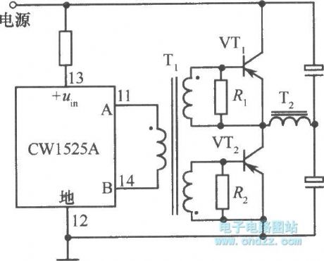
Half-bridge driver circuit of CWl525A-driven MOS tube
Published:2011/4/22 5:59:00 Author:May | Keyword: Half-bridge driver
View full Circuit Diagram | Comments | Reading(643)
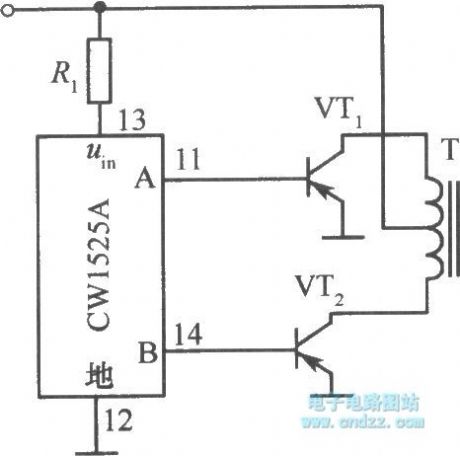
CWl525A driving bipolar half-bridge circuit
Published:2011/4/22 6:01:00 Author:May | Keyword: driving, bipolar half-bridge
View full Circuit Diagram | Comments | Reading(485)
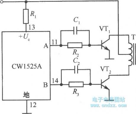
CWl525A driving bipolar push-pull circuit
Published:2011/4/22 6:01:00 Author:May | Keyword: driving, bipolar push-pull
View full Circuit Diagram | Comments | Reading(615)
CWl842 isolation driven MOS tube
Published:2011/4/22 6:04:00 Author:May | Keyword: isolation driven, MOS tube
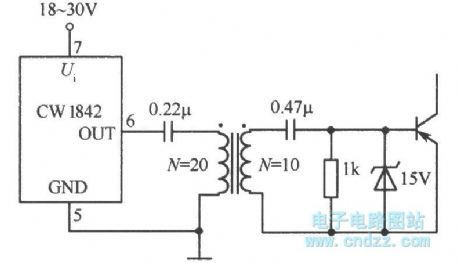
View full Circuit Diagram | Comments | Reading(455)
CWl842 directly driving M06 tube
Published:2011/4/22 6:05:00 Author:May | Keyword: directly driving, M06 tube
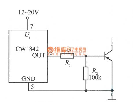
View full Circuit Diagram | Comments | Reading(494)
CWl842 directly driving bipolar type power tube
Published:2011/4/22 6:06:00 Author:May | Keyword: directly driving bipolar type, power tube
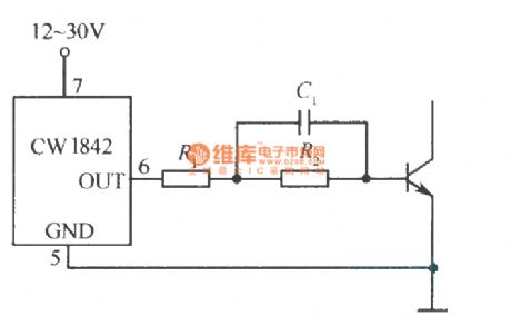
View full Circuit Diagram | Comments | Reading(444)
xTimer V1.0
Published:2011/4/25 3:20:00 Author:Ecco | Keyword: Timer
Complete schematic is shown in Fig 2. The MCU is AT89C4051 with 11.0592MHz xtal. The MAX7219 needs only three signals, CLK, DIN and LOAD. These signals are software generated assembly code. You may learn how assembly code interface with c from the firmware. Since when power up, all port bits are logic high, so I chose the 7407, open collector to provide NPN O/C output. These output bits are suitable for opto-isolator driving. The sample output module is opto-triac, the MC3040. The input circuit is simple with current mode driving, say 15mA is enough for MC3040. The output triac having ZCS drives a 220V coil electromechanical relay. Since the relay contact provide NO and NC, so we can provide two function AC plugs, i.e., delay on for NO and delay off for NC contacts.
The sample schematic shown in Fig 2. has the relay circuit that uses opto triac driving a NO/NC relay! So I must change the firmware to let the output turn on when start timer and turn off when time is over. To do such changing, it needs to modify the source code and recompile it. I thought why don't try with sdcc. The people can modify the source code and do-it-yourself. (View)
View full Circuit Diagram | Comments | Reading(500)
Night Light Saver V6
Published:2011/4/25 3:30:00 Author:Ecco | Keyword: Night Light , Saver , V6
Figure 1 shows complete hardware schematic of the Night Light Saver V6.0. The AC line was protected F1, a 1A fuse. Any short circuit caused by saver's components will blow the fuse. R1 and C1 limit current to the +5V zener diode, D3. R2 discharges capacitor C1 when power terminal of the circuit was opened. The super capacitor C2,+5V 0.01F filters DC supply. D4 acts as unidirectional switch for current supplied to MCU. BT1 is +3V 60mAH Ni-MH battery for backup the MCU when main power failed. The charging current is approx. 2mA with AC main lives. When main power failed, BT1 supplies approx. 4mA to the MCU. With fully charged, it could be able to provide backup time approx. 15Hrs. The MCU runs with +Vbackup. SW1 helps reset the MCU, in case of brownout voltage by BT1. C4 and internal pull-down resistor forms simple reset circuit. The MCU, 89C2051 runs with 3.579MHz Xtal. SW2 is for clock setting, when pressed, time will be 18:00. P3.7 drives tick LED with small sink current. R5, 4.7k limits less than one mA for D5. P3.0 provides 5Hz clock signal for calibration. The output bit is P1.6. It drives PNP transistor, Q1. R3 limits base current. R5 pull base pin to +V when P1.6 is logic '1' to fully turn off Q1. R4 limits DC current injected to Q2, MAC97 small triac. LP1 is incandescent 25W lamp. The (View)
View full Circuit Diagram | Comments | Reading(536)
| Pages:436/471 At 20421422423424425426427428429430431432433434435436437438439440Under 20 |
Circuit Categories
power supply circuit
Amplifier Circuit
Basic Circuit
LED and Light Circuit
Sensor Circuit
Signal Processing
Electrical Equipment Circuit
Control Circuit
Remote Control Circuit
A/D-D/A Converter Circuit
Audio Circuit
Measuring and Test Circuit
Communication Circuit
Computer-Related Circuit
555 Circuit
Automotive Circuit
Repairing Circuit