
Basic Circuit
Index 437
Easy-Downloader V1.1 with SDCC
Published:2011/4/25 3:27:00 Author:Ecco | Keyword: Easy-Downloader , SDCC
The hardware has a bit change at rs232 level converter. Now the circuit uses a popular rs232 level converter, MAX232. Also I cut the bridge diode at the DC input, now I use only one diode to prevent wrong polarity of a given DC adapter.
18 March 2004: found hardware schematic error at MAX232. The error is that pin 2 on the D-SUB 9 connector must be connected to pin 13 on the MAX232, not pin 8. The error had reported by Henrik Olesen, student at the University of Southern Denmark. (View)
View full Circuit Diagram | Comments | Reading(568)
MAX846A pin array diagram
Published:2011/4/25 3:26:00 Author:Nicole | Keyword: pin
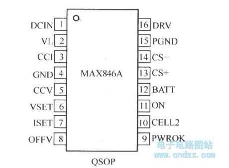
MAX846A is a low cost and multifunction battery charge controllor produced by Maxim Company, its pin array diagram is shown as below:
(View)
View full Circuit Diagram | Comments | Reading(596)
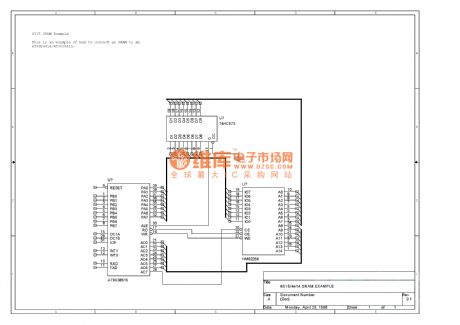
8515 extending RAM circuit diagram
Published:2011/4/25 2:46:00 Author:Ecco | Keyword: extending, RAM
View full Circuit Diagram | Comments | Reading(571)
Motor vehicle steering flasher 1
Published:2011/4/21 1:57:00 Author:Ecco | Keyword: Motor vehicle, steering flasher
(View)
View full Circuit Diagram | Comments | Reading(507)
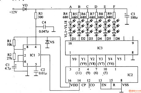
Motor vehicle steering flasher 11
Published:2011/4/21 22:07:00 Author:Ecco | Keyword: Motor vehicle, steering flasher

The motor vehicle steering flasher described in the example is a non-contact electronic flash which uses a VMOS power field effect transistor and 555 time base circuit. It has the features of long life, good effects, alternative use of magnetic motor steering and electronic flasher.
The working principle
The motor vehicle steering flasher circuit is composed of multivibrator, audio driver and flash control circuit, it is shown in Figure 7-20.
Multivibrator circuit consists of time-base integrated circuit IC, resistor Rl, saturated capacitors Cl, C2.
Audio driver circuitis composed ofthe resistor R3, transistor V, and the speaker BL.
Flash control circuit is composed of VF power field effect transistors by the VMOS, diode VDl, VD2, resistors R4, turn signal HLl-HL4 and turn signal switch S.
Component selection
RI-R4 selects 1/4W carbon film resistor or metal film resistors.
Cl selects electrolytic capacitor with voltage in 16V; C2 uses polyester capacitorsor monolithic capacitor. (View)
View full Circuit Diagram | Comments | Reading(549)
How to use 74LS138 cascaded forming 000~1FF addressing space?
Published:2011/4/25 2:39:00 Author:Ecco | Keyword: cascaded , 000~1FF , addressing space
View full Circuit Diagram | Comments | Reading(824)
Distribution diagram of each pin of p4 478 chip
Published:2011/4/25 2:20:00 Author:Ecco | Keyword: Distribution , each pin , chip
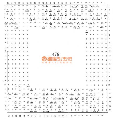
View full Circuit Diagram | Comments | Reading(552)
The hardware circuit of monolithic electronic hard disk controlled by SST89C58
Published:2011/4/25 2:23:00 Author:Ecco | Keyword: hardware circuit , monolithic, electronic , hard disk
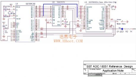
View full Circuit Diagram | Comments | Reading(854)
Serial turning Infrared circuit
Published:2011/4/25 2:27:00 Author:Ecco | Keyword: Serial , turning , Infrared
View full Circuit Diagram | Comments | Reading(537)
at89c51 DIY Programmer(English)
Published:2011/4/25 2:10:00 Author:Ecco | Keyword: DIY , Programmer
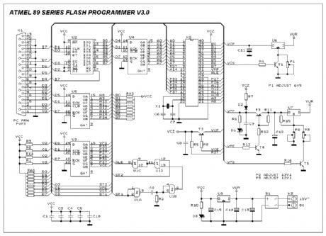
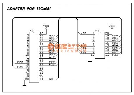
Figure 1 shows the circuit diagram of the Flash Programmer, the programmer is interfaced with the standard parallel port of the PC. As shown in the diagram U2 is used to control the data flow between the controller and the PC, U4 latched the low order address byte and U5 latched the high order address byte, while U3 is used to generate the control signals for micro controller to be programmed. IC U1 is used to generate the progrram pulse for the u-controller. The power supply section uses U8 to generate the logic 5V supply while the U7 is used to provide the programming supply voltage to controller. IC U6 is used to generate the VDD power supply voltage for the u-controller which is selectable either 5v or 6v5.
The power to the circuit is provided by a wall adapter of 15 to 18V output, normally a 15V type adapter will provide a 19~20V output voltage. As shown in the diagram the crystal X1 can be replaced by a resonator in that case capacitors C4 and C5 are not required. Place a small heatsink on U8 voltage regulator.
For the adjustment of P1, P2 and P3 use a digital multimeter & follow the steps shown below,
1. To adjust P1, temporarily connect T1 base to ground using test clips then adjust P1 to get 6.5V at the output of regulator U6.2. Next first adjust P2 to get the 13.1V at the output of regulator U7, make sure transistor T5 is off or temporarily connect the T5 base to ground using test clips.3. Now temporarily short the collector of transistor T5 to ground using test clips.3. Adjust P3 to get the 12.1V at the output of U7 regulator IC.
Figure 2 shows the circuit diagram of the interface adapter card required for the programming of 20 pin Flash devices.
Pgm89v3.zip file is used to run the programmer. This is a Windows program which can be used underWindows 95 & 98. The main screen of the program is shown in figure 4.
In order to insure safe insertion & removal of the u-controller from programmer ZIF socket make sure programmer power supply is turned on before starting the program and the red LED D1 must be turned off when the program is started. The u-controller should be placed or removed from the ZIF socket when the red LED D1 is off.Also note that the software does not provide the erase command because this function is performed automatically during device programming. If you are required to erase the controller first use the clear buffer command in edit menu then program the controller, this will erase the controller memory. (View)
View full Circuit Diagram | Comments | Reading(4885)
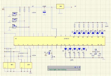
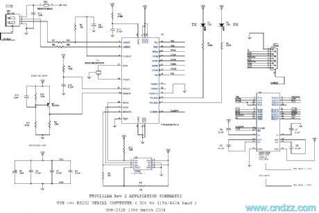
at89c2051 DIY Programmer(English)
Published:2011/4/25 2:17:00 Author:Ecco | Keyword: DIY , Programmer
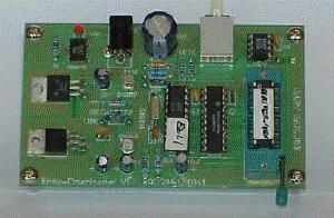
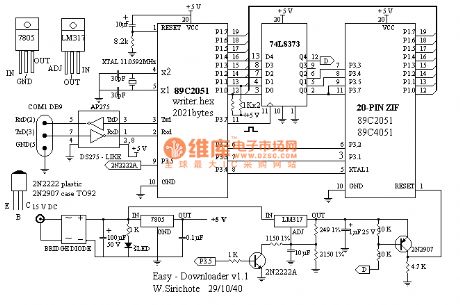
Figure 1 depicts a circuit diagram of the Easy-Downloader. As shown, the circuit uses a 89C2051 with writer.hex firmware, 74LS373 8-bit latch, DS275-like, 7805, LM317 and two transistors, 2N2222A and 2N2907A. The programming voltage control circuit is the same as recommended by ATMEL application note. It can be raised from 0V, 5V and 12V by appropriated signal from P3. The 8-bit latch, 74LS373 provides some signal for selecting the programming modes. A byte to be programmed or read back is sent/received through P1. Incrementing address is done by pulsing a positive pulse to XTAL pin. The circuit may be built using simple point-to-point soldering with a general purpose PCB( fish's egg like PCB) or making PCB shown above, the file is Easy-v1.pcb Protel PCB version 2.76. The finished board should be tested without any chips; 1) +5V supply, 2) programming voltage 0V, 5V and 12V by connecting the pin that control (P3.5 and D) 2N2222A and 2N2907 to +5V and/or GND. The adapter output should be approx. 15Vdc 100mA.
(View)
View full Circuit Diagram | Comments | Reading(3431)
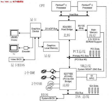
440bx mainboard structure chart
Published:2011/4/25 1:49:00 Author:Ecco | Keyword: mainboard, structure
View full Circuit Diagram | Comments | Reading(1110)
24cxx reproducer circuit
Published:2011/4/25 1:47:00 Author:Ecco | Keyword: reproducer
View full Circuit Diagram | Comments | Reading(964)
The XC4003 minimum system circuit
Published:2011/4/25 1:46:00 Author:Ecco | Keyword: minimum system
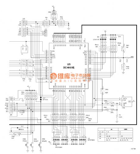
View full Circuit Diagram | Comments | Reading(697)
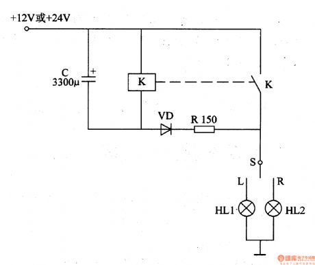
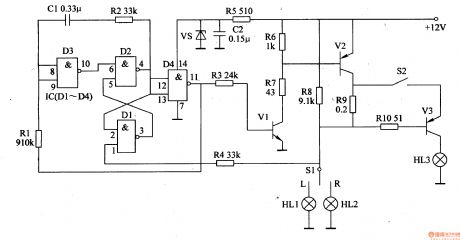
Motor vehicle steering flasher 10
Published:2011/4/21 21:38:00 Author:Ecco | Keyword: Motor vehicle , steering flasher

The working principle
The motor vehicle steering flasher is composed of capacitor C, the relay K, diode VD and resistors R, it is shown in Figure 7-19.
When the turn signal switch S is placed in L (or R position), C begins charging, and the left turn signal HLl (or right turn signal HL2) is lit. With the gradually increasing voltage of C, HLl (or HL2) light fades, when the voltage of C reaches the pull-in voltage of K, K pulls in, and its normally open contact is connected, at this time , the brightness of HLl (or HL2) is largest. Then C discharges through K, when the voltage of C voltage declines down to the releasing voltage of K, K releases, HLl (or HL2) is off. When C starts charging, HLl (or HL2) is lit again, and the circuit repeats the process.
Adjusting the resistance of R can change the note selection of turn signal flash rate.
R uses 1/2W metal film resistors.
C uses electrolytic capacitor with voltage in 35V.
VD selects 1N4001 or 1N4007 silicon rectifier diodes.
K uses 24V or 12V DC relay with the contact current capacity greater than IOA.
(View)
View full Circuit Diagram | Comments | Reading(1031)
Motor vehicle steering flasher 9
Published:2011/4/21 21:21:00 Author:Ecco | Keyword: Motor vehicle, steering flasher
The motor vehicle steering flasher described in the example uses discrete components, and it has the features of low cost and easy to produce, stable performance, it can be used for motorcycle or car.
The working principle
The motor vehicle steering flasheris composed ofthe flash circuit resistors Rl-R3, capacitor Cl, C2, the transistor V, diode VD and relays K, it is shown in Figure 7-18.
Whenturning signal switch S (in the center), V does not work, K isin the releasing state, HLland HL2are notflashing.
Component selection
Rl uses 2w insurance resistors;
R2 and R3 select 1/4W metal film resistor or carbon film resistors.
Cl uses electrolytic capacitor with voltage in 16V; C2 uses polyester capacitor or CBB capacitor.
V uses S8550 silicon PNP transistor.
VD uses IN4007 silicon rectifier diode.
K selects 4098 DC relay.
(View)
View full Circuit Diagram | Comments | Reading(509)
A simple 485 card circuit diagram
Published:2011/4/25 1:22:00 Author:Ecco | Keyword: simple, 485 , card
View full Circuit Diagram | Comments | Reading(502)
Usb mouse circuit diagram
Published:2011/4/25 1:33:00 Author:Ecco | Keyword: Usb mouse
View full Circuit Diagram | Comments | Reading(3348)
AMD462 CPU circuit diagram
Published:2011/4/25 1:29:00 Author:Ecco | Keyword: CPU
View full Circuit Diagram | Comments | Reading(623)
Motor vehicle steering flasher 8
Published:2011/4/21 21:08:00 Author:Ecco | Keyword: Motor vehicle , steering flasher
The working principle
The motor vehicle steering flasher is composed of pulse generator and electronic switching circuit, it is shown in Figure 7-17.
Pulse generator circuit consists of NAND gate integrated circuit IC (Dl-D4), voltage regulator diode VS, resistors Rl, M, M, R5 and capacitors Cl, C2.
Electronic switching circuit consists of resistors R3, R6-RlO and transistors Vl-V3.
Sl is a vehicle turn signal switch, S2 is the door flashes light switch. HLl is the left turn signal, H is the right turn signal, HL3 is flashing lights.
+ L2V voltage is limited by R5, filtered by C2 and regulated by VS to provide IC +9 V voltage.
Component selection
Rl-R4, R6, R7 and RlO use 1/4W carbon film resistor or metal film resistors; R5 and R8 select 1/2W metal film resistors; R9 uses 5-lOW insurance resistor.
Cl and C2 chose monolithic capacitors or polyester capacitors.
VS selects lW, 9V silicon voltage-regulator diode.
Vl uses S9013 or S8050 silicon NPN transistor; V2 use 5OV silicon PNP transistors with the current higher than 5A, for example 3CA8B, BD246A or 2SA807,etc.; V3 chooses 5OV, 2A silicon PNP transistors, for example 2SAl213, 3CA4, 3CA6,etc.
IC uses CD401l or CC401l, MCl4011 NAND gate integrated circuits.
S2 chooses single pole switch with the current of contacts being over 5A.
(View)
View full Circuit Diagram | Comments | Reading(583)
| Pages:437/471 At 20421422423424425426427428429430431432433434435436437438439440Under 20 |
Circuit Categories
power supply circuit
Amplifier Circuit
Basic Circuit
LED and Light Circuit
Sensor Circuit
Signal Processing
Electrical Equipment Circuit
Control Circuit
Remote Control Circuit
A/D-D/A Converter Circuit
Audio Circuit
Measuring and Test Circuit
Communication Circuit
Computer-Related Circuit
555 Circuit
Automotive Circuit
Repairing Circuit