
Basic Circuit
Index 421
DC isolation circuit daigram with harmonic suppression
Published:2011/5/11 4:00:00 Author:Ecco | Keyword: DC , isolation, harmonic suppression
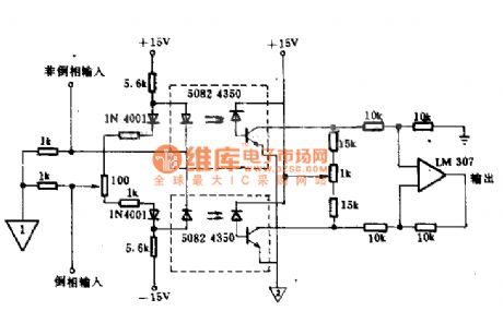
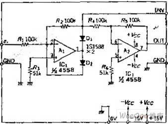
This circuit uses two isolators to reduce the harmonic generation as the working of push-pull amplifier. When it is coupled with the input signal, the gain of one isolation tube will increase, another isolation tube reduces for compensation, then it eliminates harmonics. The gain of the circuit is about 1. When the signal is less than 2 rounds (peak - peak), the bandwidth is 2MHz. The inverting or non-inverting input end can be added any polarity input signal.
(View)
View full Circuit Diagram | Comments | Reading(1110)
Digital voltmeter circuit diagram with single + 5V power supply composed of ICL7107
Published:2011/5/11 3:00:00 Author:Ecco | Keyword: Digital , voltmeter , single, + 5V , power supply
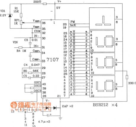
Digital voltmeter circuit diagram with single + 5V power supply composed of ICL7107 3 1 / 2 double integral A / D converter is shown as the chart.
(View)
View full Circuit Diagram | Comments | Reading(11764)
Digital voltmeter circuit diagram composed of ICL7106
Published:2011/5/11 2:57:00 Author:Ecco | Keyword: Digital voltmeter
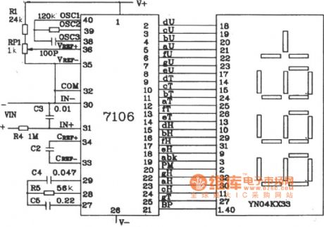
Digital voltmeter circuit diagram composed of ICL7106 3 1 / 2 double integral A / D converter is shown as the chart.
(View)
View full Circuit Diagram | Comments | Reading(16863)
Digital capacitance table circuit diagram composed of ICL7107
Published:2011/5/11 2:31:00 Author:Ecco | Keyword: Digital capacitance table
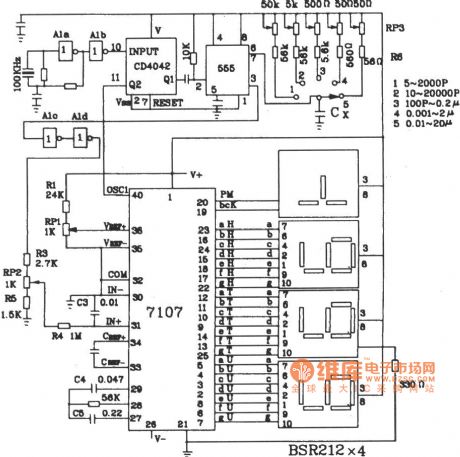
Digital capacitance table circuit diagram composed of ICL7107 is shown as the chart.
(View)
View full Circuit Diagram | Comments | Reading(7630)
Polymer capacitances-type humidity sensor application circuit
Published:2011/5/10 1:14:00 Author:Fiona | Keyword: Polymer capacitances-type, humidity sensor
Illustration is polymer capacitances-type humidity sensor application circuit.It consists of two time base circuit IC1,IC2 composition.IC1 and external components compose themultivibrator which mainly triggers IC2 's pulse.ICz,capacitance-type humidity sensor and external component compose theadjustable wide pulse generator .The pulse width will depend on the humidity sensor capacitance size.The width pulse output from the IC2's ⑨ feet,filtered by R5, C3, then put out as DC signal.It is proportional to the air'srelative humidity, the sensitivity of 2mv /% RH.
(View)
View full Circuit Diagram | Comments | Reading(529)
Resistance-type condensation sensor application circuit
Published:2011/5/10 1:12:00 Author: | Keyword: Resistance-type, condensation sensor
Illustration is resistance-type condensation sensor application circuit .Shown in figure (a) is positive characteristics condensation sensor application circuit and Shown in figure (b) is negative characteristics condensation sensor application circuit. (View)
View full Circuit Diagram | Comments | Reading(521)
Metal oxides humidity sensor application circuit
Published:2011/5/10 1:00:00 Author: | Keyword: Metal oxides, humidity sensor
The low-frequency oscillator is composed&nbs (View)
View full Circuit Diagram | Comments | Reading(460)
universal single and dual power supply quad op-amp circuit
Published:2011/5/9 2:00:00 Author:John | Keyword: quad op-amp

LM324 is a high-gain quad op-amp, which has four modules inside. Both single power and dual power supply are available for operating. It can work under a rather wide range of working power supply voltage. A very small Supply Current is needed. Input bias current is with temperature compensation performance, so no external frequency compensation components are needed. Amplifier LM324 can be applied in conversion amplifiers, DC gain units and universal op-amp circuits for many applications. And it also can be used directly as interface circuit for a variety of logic circuits and other low-pressure systems. Direct models or substitutions can be LMl24、CFl24MD、CF224LD、CFl24MJ、CF224LJ、CF324CJ and CF324CP and so on. The circuit shown above is the situation that LM324 is used as a dual-threshold voltage comparator.
(View)
View full Circuit Diagram | Comments | Reading(1183)
C271AD single-chip micro-computer communication integrated circuit diagram
Published:2011/5/10 1:16:00 Author:Fiona | Keyword: single-chip micro-computer communication
C271AD is a single-chip micro-computer communication integrated circuit. It's widely used in wireless phones and other communication devices.
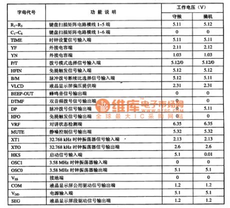
1. Features
C271AD integrated circuit's in-circuit is mainlyformed by the key position pulse generator circuit, the key instruction encoding circuit, the clock oscillation circuit, two-tone and pulse signal processing circuit,pulse dialing rate intermittent selection circuit,dial-up mode selection circuit, hands-free control circuit, squelch Control circuit etc.
2. pin functions and data
C271AD related pin letter designations, function descriptions and data are listed in Table 1.
Table 1 C271AD integrated circuit's pin functions and data
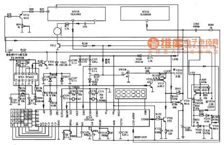
3. Typical application circuit
the control system typical application circuit which isformed by the C271AD integrated circuit is shown in Figure 1.
Figure 1 The typical application circuit of the C271AD integrated circuit
(View)
View full Circuit Diagram | Comments | Reading(1516)
universal single-supply dual operational amplifier circuit
Published:2011/5/10 23:07:00 Author:John | Keyword: single-supply, dual operational amplifier
(View)
View full Circuit Diagram | Comments | Reading(884)
Universal Dual Power Dual op-amp circuit
Published:2011/5/10 23:07:00 Author:John | Keyword: Dual Power, Dual op amp

Operational amplifiers CF1458 series are amplifiers with high performance dual op amp, whose electrical performance is the same with that of the amplifier /-A747. But the arrangement of pin for these series is different from each other.The features of these series are listed in the following. No external frequency compensation components are needed. And the amplifiers are provided with short circuit protection and the ability to offset voltage to zero. Besides, there is a wide input voltage range for differential mode and common mode. It has low power consumption and no obstruction. Substitutions or direct models can be amplifiers CF1558MT, CF1458CT, CF1558NMT, CF1458NCT, CF1558SMT, CF1458SCT, CF1558MD, CFl458CD, CFl558MJ, CFl458cJ, CFl458CP, CFl558NMD, Fl458NCD, CFl558SMJ, CFl458SCJ, CFl458SCP, CFl558SMD and so on. Amplifiers CFl458N and CFl558N are able to work with low noise. And amplifiersCFl458S and CFl558S can work with high conversion rate. (View)
View full Circuit Diagram | Comments | Reading(926)
Availability of positive and negative output ideal diode circuit
Published:2011/5/10 1:11:00 Author: | Keyword: Availability of positive and negative output


Circuit function
The common diode has forward voltage drop and can not do tiny signal rectifier, and when the signal amplitude is large, if the ambient temperature increases, the rectifier voltage will change with it,it is difficult to form high-precision circuit. Ideal diode circuit can get zero diode characteristic.This circuit can be realized by the feedback circuit of OP amplifier.
Circuit work
OP amplifier A1 is the negative output's ideal diode circuit, cascades diode D1 with the output and starts to feedback from the positive of D1.In terms of the positive input signal , A1 only plays the role of a simple inverting amplifier.
When negatively inputs, OP amplifys the output of A1 to be positive, D1 is disconnected.In order to ensure the circuit works in the open-loop state and to prevent saturation, it also cascades diode D2 with the output. The positive output of A1 is clamped by diode forward voltage drop. OP Amplifier A2 is a inverting amplifier that the magnification is 1,whose function is to reverse the output of A1. If using a unipolar output, the A2 removes. Circuit R3, R6 's function is using the bias current IE of the OP amplifier's inputto eliminate offset voltage, if choosing the FET input OP amplifier ,it can be removes R3, R6.
(View)
View full Circuit Diagram | Comments | Reading(833)
The basic connection circuit of INAL25 signal and power supply
Published:2011/5/8 18:44:00 Author:Christina | Keyword: basic connection, signal, supply
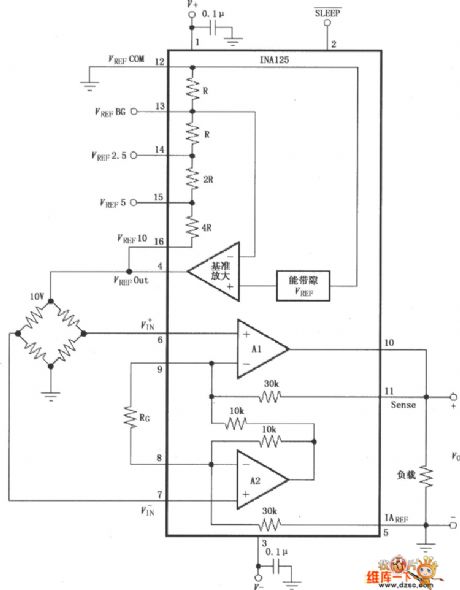
The The basic connection circuit of INAL25 signal and power supply is as shown. In the noise environments or high-impedance power supply applications, the chip power port need to use the capacitor filter, and close to the chip power pin. The output voltage is based on the iaref port standard. You should notice that the standard terminal need to be low resistance connection to ensure the CMRR is high, such as if there is a 12ω series resistance, the CMRR will decrease about 80db(g=4). Gain g=4+60kω/rg, in this formula, 60kω means the total value of the two internal feedback resistors of ina125. The two internal feedback resistors are regulated by the laser, so the selection of external resistor rg has great impact with the gain, you need to use the resistance of good stability and small temperature drift. When the circuit needs to work in the high gain state, the external resistor rg's value is small, you should notice the contact resistance of lead, such as if the socket contact is good.etc, the lead's contact resistance direct results the gain error and affects the stability.
(View)
View full Circuit Diagram | Comments | Reading(638)
Non-source adjustable constant electronic load circuit
Published:2011/5/10 22:34:00 Author:Christina | Keyword: Non-source, adjustable, constant electronic load
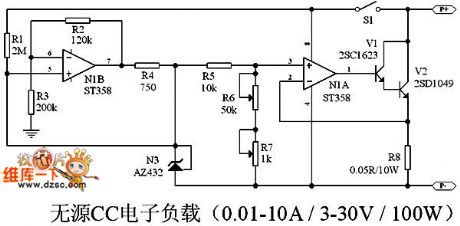
In power supplier industry, the electronic load is the necessary R&D or production equipment of all manufacturers, most electronic loads in the market are very expensive, and they need the power supplier to work. This article supplies one kind of circuit scheme, so that the readers can make the CC mode passive adjustable electronic load by themselves, the input voltage range is 3 to 30V, the input current range is 0.01A to 10A.
The circuit is as shown:
S1 is the load switch, you can disconnect the whole load by S1.
N1B is the quasi-constant current source circuit, the N1B can make the 432 toproduce the1.25V standard and it can also make the current of 432 unchanged even if the input voltage changes. In the CC mode, R8 is the current sampling resistor to feedback the current and make the load current constant. Resistance R6 is the coarse adjustment resistor, resistance R7 is the fine adjustment resistor. (View)
View full Circuit Diagram | Comments | Reading(8290)
Electrical bridge circuit
Published:2011/5/10 8:32:00 Author:Christina | Keyword: Electrical bridge
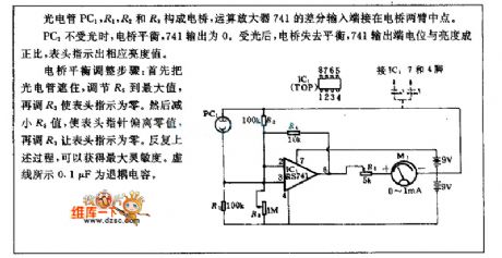
The Electrical bridge circuit is as shown:
The E-bridge is composed of the phototube PC1, R1, R2 and R3, the operational amplifier 741's differential input port connects to the middle-point of the E-bridge's two arms.
When the PC1 has no light, the e-bridge is balance, the output of 741 is 0. When the PC1 has light, the e-bridge is out of balance, the electric potential of 741 output port is proportional to the brightness, the header indicates the corresponding brightness value.
The bridge balance adjustment step: first you need to cover the photocell, then adjust R5 to the maximum value, and adjust R3 to make the meter indicates to zero. Then decrease the value of R5 to make the pointer deviation from zero, and adjust R3 to make the meter indicates to zero. Repeat this process and you can get the maximum sensitivity. The dotted line showns the 0.1uF decoupling capacitor. (View)
View full Circuit Diagram | Comments | Reading(695)
Practical band-pass filter principle circuit diagram
Published:2011/5/10 22:19:00 Author:Nicole | Keyword: band-pass filter
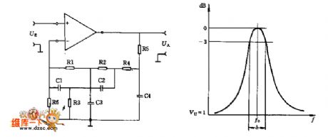
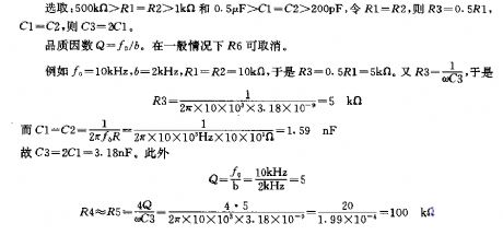
In negative feedback branch, this circuit is a bandstop filter, then it only allow the frequency singal which is blocked down by feedback branch to pass.
(View)
View full Circuit Diagram | Comments | Reading(728)
Usual band-pass filter circuit diagram
Published:2011/5/10 22:25:00 Author:Nicole | Keyword: band-pass filter
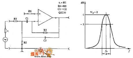
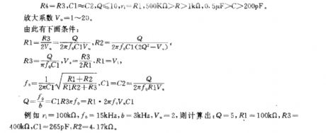
In this circuit, the R1 value is decided beforehand, the value is similar to the singal source internal resistance r. The principle of parameters selection is:
(View)
View full Circuit Diagram | Comments | Reading(676)
Unipolar reversed circuit diagram composed of ISO100
Published:2011/5/10 21:29:00 Author:Ecco | Keyword: Unipolar , reversed
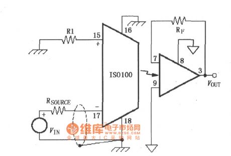
Unipolar reversed circuit diagram composed of ISO100 is shown as the chart. The circuit is a reversed amplifier, which can enlarge the unipolar input signal VIN, it requires VIN ≥ 10μA × Rsource to ensure the normal work of internal LED, photodiode, of which Rsource is internal resistor of the signal source. Inverting amplifier gain is decided by the RF, R1, that is, VOUT =- VIN (RF/R1).
(View)
View full Circuit Diagram | Comments | Reading(520)
Unipolar mode noise reducing method circuit diagram composed of ISO100
Published:2011/5/10 20:46:00 Author:Ecco | Keyword: Unipolar mode , noise reducing method
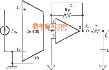
Unipolar mode noise reducing method circuit diagram composed of ISO100 is shown as the chart. In the unipolar mode, the noise is produced primarily by the conductive hole of optical components. If it does not need to work in the whole frequency range of 60kHz, the feedback loop can be added a capacitor CF to limit the output noise, and it would get a better effect while adding a RC low-pass filter.
(View)
View full Circuit Diagram | Comments | Reading(659)
Typical Applied Circuit of M52340SP IC
Published:2011/5/10 19:32:00 Author: | Keyword: IC, Applied Circuit
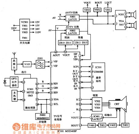
Typical Applied Circuit
The typical applied circuit of M52340SP IC is demonstrated as the abboved picture.Konka F2136 color TV is a typical application example.
Picture:Typical Applied Circuit of M52340SP IC
Note:Ifboth image and sound accompaniment go wrong meanwhile ,we shuold check 38MHz intermediate sequancy signal which is high sequancy singalat first but changed into intermediate then whether it is added to⑥ and ⑦ feet.The M52340SPcircuit will be checked if the signal is normal. (View)
View full Circuit Diagram | Comments | Reading(857)
| Pages:421/471 At 20421422423424425426427428429430431432433434435436437438439440Under 20 |
Circuit Categories
power supply circuit
Amplifier Circuit
Basic Circuit
LED and Light Circuit
Sensor Circuit
Signal Processing
Electrical Equipment Circuit
Control Circuit
Remote Control Circuit
A/D-D/A Converter Circuit
Audio Circuit
Measuring and Test Circuit
Communication Circuit
Computer-Related Circuit
555 Circuit
Automotive Circuit
Repairing Circuit