
Basic Circuit
Index 423
74 series digital circuit 74LS538 3-8 line demultiplexe(three states)
Published:2011/5/9 22:32:00 Author:Nicole | Keyword: 74 series, demultiplexe
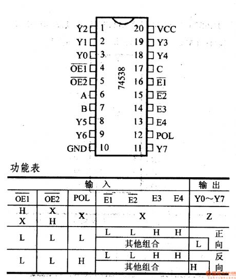
74LS538, 74F538, 3-8 line demultiplexe(three states)
It can switch the positive output or negative output; it has three states output.
(View)
View full Circuit Diagram | Comments | Reading(1061)
Very simple low pass filter(integrator) circuit diagram
Published:2011/5/10 1:45:00 Author:Nicole | Keyword: low pass filter, integratorv
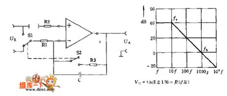
It is a simple low pass filter, it also can be used as integrator, when it is used as integrator, the switch S1 is connected to input terminal, and S2 is cut off. When it is used as low pass filter, R3 is connected to circuit, then the voltage amplification is Vo=R3/R1, the singal source internal resistance Ri << R1, and R2's value should be equal to the parallel equivalent value of R3 and R1.
The frequency value is determined by the below formula:
(View)
View full Circuit Diagram | Comments | Reading(832)
One dimension PSD equivalent circuit diagram
Published:2011/5/10 2:52:00 Author:Nicole | Keyword: one dimension, PSD equivalent

View full Circuit Diagram | Comments | Reading(645)
Ordinary filter circuit diagram
Published:2011/5/10 2:43:00 Author:Nicole | Keyword: filter
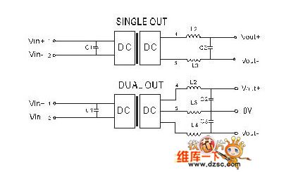
In the ripple and noise susceptible circuit, it can add a filter to DC/DC input terminal and output terminal, it can reduce the ripple and noise. It can absorb the peak voltage of input terminal by importing additional capacitance, it also can store energy and keep voltage stable, The output ripple can be reduced by exporting additional capacitance, the capacitance value too large or ESR too low will easily cause start up problems; if it requires very low ripple, it can adopt LC filtering network or use power module with low ripple output.
(View)
View full Circuit Diagram | Comments | Reading(1291)
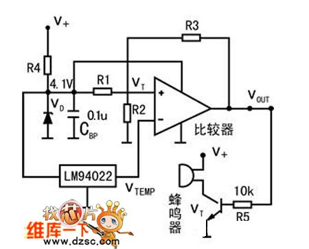
Simple excess threshold temperature alarm circuit diagram
Published:2011/5/10 3:17:00 Author:Nicole | Keyword: threshold temperature
View full Circuit Diagram | Comments | Reading(581)
Common active power filter circuit diagram with steady performance
Published:2011/5/9 22:16:00 Author:Nicole | Keyword: active power filter, steady performance
The circuit is as shown, the new frequency fo=3.4KHz, the notch frequency fo=9.5KHz, the quality factor Q=3.4. For high frequency filter, the transfer coefficient is 0.1, for band-pass filter, it is 1, for low frequency filter, it is 1, for notch filter, it is 10. foQ≤200KHz, when the output sine signal is within 10V, the maximum frequency is no more than 200KHz.
(View)
View full Circuit Diagram | Comments | Reading(938)
Digital frequency meter circuit diagram composed of ICL7107
Published:2011/5/9 22:05:00 Author:Ecco | Keyword: Digital , frequency meter
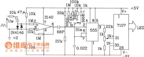
Digital frequency meter circuit diagram composed of ICL7107 is shown as the chart.
(View)
View full Circuit Diagram | Comments | Reading(7570)
Metal oxides humidity sensor application circuit diagram
Published:2011/5/9 2:31:00 Author: | Keyword: Metal oxides, humidity sensor
The low-frequency oscillator is composed&nbs (View)
View full Circuit Diagram | Comments | Reading(511)
Resistance-type condensation sensor application circuit diagram
Published:2011/5/9 2:31:00 Author: | Keyword: Resistance-type, condensation sensor
Illustration is resistance-type condensation sensor application circuit .Shown in figure (a) is positive characteristics condensation sensor application circuit and Shown in figure (b) is negative characteristics condensation sensor application circuit. (View)
View full Circuit Diagram | Comments | Reading(431)
Strain bridge current transmitter circuit diagram composed of XTR115 precision current transmitter
Published:2011/5/6 2:47:00 Author:Ecco | Keyword: Strain bridge, current transmitter , precision
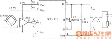
Strain bridge current transmitter circuit composed of XTR115 is shown as the chart. Pin 3 will be regarded as public place, pin 1 will provide +2.5 V power supply to the strain bridge. Pre-amplifier uses TL061 single op amp (also uses OPA2277 dual op amp, only one op amp), the +5 V regulator will provide power the op amp by itself. R1 is 20kΩ input resistor, C is the noise reduction capacitor, VT is the external NPN power transistor, which can select 2N4922, TIP29C, TIP31B models. it set 2N4922 as an example, the main parameters UCEO = 60V, ICM = 1A, PCM = 30W. The circuit working principle: when the force is on the specimen, the voltage signal output by strain bridge firstly passes through the pre-amplifier and changes into the 0.8 ~ 4V input voltage UI, and then it is input current of 40μA ~ 200μA II converted by the RI, at last it will be amplified 100 times by the XTR115 and obtains 4 ~ 20mA current.
(View)
View full Circuit Diagram | Comments | Reading(2555)
Chip diode appearance circuit diagram
Published:2011/5/9 21:41:00 Author:Ecco | Keyword: Chip diode , appearance
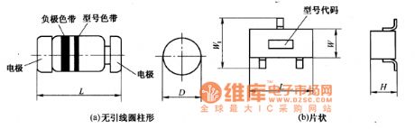
Chip diode appearance circuit diagram is shown as the chart.
The chip diode has many different types such as the rectifier diode, varactor diode, fast recovery diode, switching diode, zener diode, light emitting diode and transient voltage suppression diode. Most models of the chip diodes use the model of leading diode, some manufacturers also have their own requiring model, There is no uniform requirements.
(View)
View full Circuit Diagram | Comments | Reading(692)
T0P2O2YA1 PWM monolithic integrated circuit diagram
Published:2011/5/9 1:37:00 Author:Ecco | Keyword: PWM , monolithic , integrated circuit
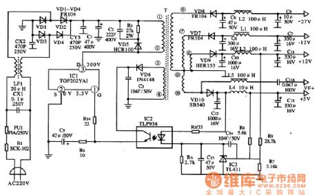
T0P2O2YA1 is the PWM monolithic switching power supply integrated circuit which is manufactured by the Power Company in the United States, it is widely used in switching power supply circuit of DVD, VCD, etc. DVD players, computers and monitors, air conditioner control system and various other household appliances. 1. pin functions and data T0P2O2YA1 IC uses separate three-pin package, the pin functions and data are listed in Table. T0P223Y integrated circuit pin functions and data 2. The typical application circuit The block diagram of T0P2O2YA1 integrated circuit and typical application circuit are shown as the chart. The block diagram and typical application circuit of T0P2O2YA1 IC
(View)
View full Circuit Diagram | Comments | Reading(1294)
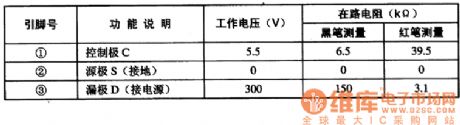
TMS34541NL-R digital clock integrated circuit diagram
Published:2011/5/9 2:07:00 Author:Ecco | Keyword: digital clock , integrated circuit
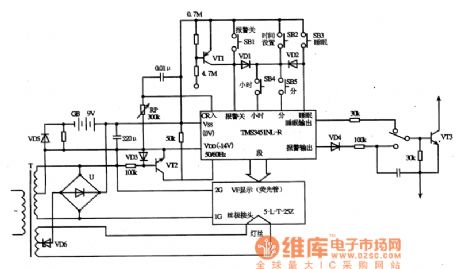
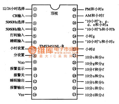
TMS34541NL-R is the digital clock integrated circuit produced by Toshiba, it is widely used in various digital clock. 1. Features of functionsTMS34541NL-R IC is mainly composed of the internal clock oscillator circuit, divider circuit, time control circuit, the comparator circuit and the fluorescent tube display output decoder and driver circuit. 2. Pin functionsTMS34541NL-R IC uses 28-pin dual in-line package, the pin functions are shown as the chart. 3. The typical application circuit The typical application circuit composed of TMS3451NL-R integrated circuit is shown as the chart.
(View)
View full Circuit Diagram | Comments | Reading(2446)
Typical applied Circuit Diagram of M54123 Intergrated Circuit
Published:2011/5/9 19:29:00 Author: | Keyword: Intergrated Circuit
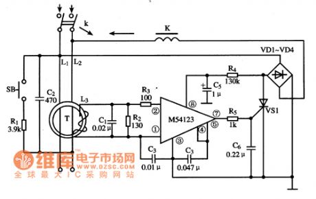
Typical Applied Circuit Diagram
Typical applied circuit diagram of leakage protecter composed of M54123 IC is demonstrated as the abboved picture.
Picture:The typical applied circuit diagram of M54123 IC
Note:China's homegrown part number of M54123 IC is SF4123 and they can be used interchangeably directly. (View)
View full Circuit Diagram | Comments | Reading(3014)
High precision remote temperature measurement circuit
Published:2011/5/7 13:07:00 Author:John | Keyword: reemote temperature measurement circuit
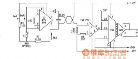
Precision temperature measurement circuit composed of ISO120 and XTR101 is mainly used in remote temperature measurement with a high temperature measurement accuracy. It can also be used for situations with strong noise. ISO120 is a new isolation amplifier, which is designed through the duty factor modulation / demodulation technology. Isolation layer is a two-matched lpF differential capacitor. Digital signals are transmitted. Transmittion of digital signal will not affect the integrity of signals caused by the isolated components. It also has a rather good high-frequency transient performance. Figure shows precision temperature measurement circuit constituted by ISO120 and XTR101. Low temperature drift XTR101 is a 4 ~ 20mA transmitter, and RTD is a thermal resistance. Circuit parameters can guarantee the output current at 4mA in the low temperature end and at 20mA in the high temperature end. Twisted pair will transforme the current to INA105. The current will be converted into electrical signals, then be output through ISO120. (View)
View full Circuit Diagram | Comments | Reading(1230)
input end zero circuit
Published:2011/5/8 2:51:00 Author:John | Keyword: input end zero circuit
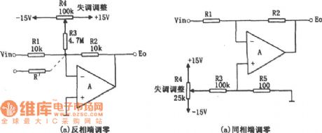
Figure (a) is a relatively simple circuit, which uses the input resistors R1 and feedback resistor R2 as one part of the attenuation, together with the resistor R3 at the inverting input in order to generate a variable offset voltage. The voltage is divied from the R3 and R1 ∥ R2. ± 15V power supply is connected at both ends of the potentiometer R4. And the partial pressure ratio is about 1000 / 1. So the offset voltage can be ranged within ± 15mV . For Figure (a), the general formul for calculating adjustment range of the offset voltage is:
offset voltage range = ± VD • [(R1 ∥ R2) / R3] (± VD = ± 15V)
When there are multiple input signals on the the reverse side, the offset voltage ranges just as shown in virtual display line of Figure (a).
multiple input offset voltage range = ± VD [(R1 ∥ R2 ∥ Rl ') / R3] (± VD = ± l5V) Comparing the above two equations, the former one is clearly with a wider voltage range of adjustment voltage. To increase the voltage adjustment range of the latter one, it is suggested to appropriately change the size of resistor R5.
Figure (b) shows that this circuit has a wide range of applications, because the adjustment voltage has nothing to do with feedback components. And adjustment voltage is set in both input ends, avoiding the winning stream signaling pathways. In this circuit, R3 and R5 of the resistance (100kΩ, 100Ω) form 1000 / I of the voltage divider. And R5 will get adjustment range of ± 15mV offset voltage at both ends. When R3 and R5 are set at other values, adjustment range of offset voltage can be determined by the following formula: offset voltage adjustment range = ± VD • (R5/R3) (± VD = ± l5V)
There is few requirements for resistance of resistors R3 and R5. In fact, it is better to choose the resistance of resistor R5 below 1kΩ. (View)
View full Circuit Diagram | Comments | Reading(908)
The interface circuit
Published:2011/5/6 3:53:00 Author:Ecco | Keyword: interface circuit
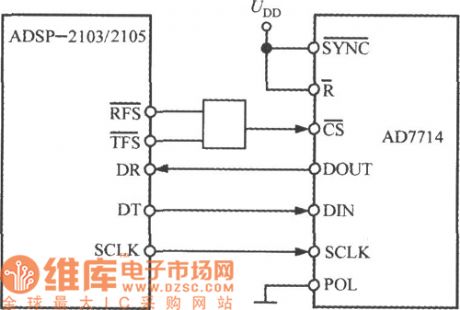
ADSP-2103 or ADSP-2105 is the digital signal processor produced by ADI. The interface circuit between AD7714 and ADSP-2103/2105 is shown as the chart. When the ADSP-2103/2105 NOT sum TES end is set in low level, the output is valid, the SCLK output is configured as serial clock terminal. POL termination of AD7714 is connected to low level. In order to ensure the AD7714 work normally, the serial clock frequency of ADSP-2103/2105 should be limited to less than 3MHz.
The interface circuit between AD7714 5-channel low-power programmable sensor signal processor and DSP (View)
View full Circuit Diagram | Comments | Reading(619)
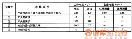
The typical application circuit diagram of PT2124 IC
Published:2011/5/9 3:42:00 Author:Ecco | Keyword: typical application circuit , IC
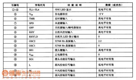
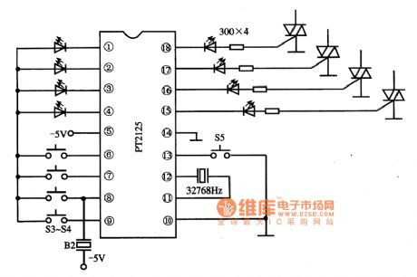
PT2125 is the fan monolithic microcomputer integrated circuit, which is widely used in various types of program control circuits. PT2125 IC uses the 18-pin dual in-line package, the pin functions and data are listed in table, it usually forms remote control fan system with the BA5101/A5201, the typical application circuit is shown as teh chart.
(View)
View full Circuit Diagram | Comments | Reading(2010)
STR-6654 thick film switching power supply integrated circuit diagram
Published:2011/5/6 4:47:00 Author:Ecco | Keyword: thick film , switching, power supply , integrated circuit
STR-6654 is the switching power supply thick film integrated circuit produced by Sanyo, it is widely used in rear projection color TV (for example, Changhong HP Series precision ), DVD players and other switching power supply circuits. 1. Features of functionSTR-6654 IC includes start circuit, driver circuit, switching adjusting tube, over-voltage protection circuit, over-current protection circuit and other ancillary functions circuit. 2. Pin functions and data STR-6654 IC uses 5-foot single-line package, the pin functions and data are listed in Table. The data is measured in Changhong HP Series of precision rear projection color TV. STR-6654 integrated circuit pin functions and data
(View)
View full Circuit Diagram | Comments | Reading(2616)
PQ3RD13 3.3V four-terminal voltage regulator integrated circuit diagram
Published:2011/5/9 3:12:00 Author:Ecco | Keyword: 3.3V, four-terminal , voltage regulator, integrated circuit
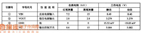
PQ3RD13 is the 3.3V controlled voltage regulator four-terminal integrated circuit, which is widely used as voltage regulator in DVD players, color, computer monitors, printers, fax machines, and a variety of household electrical power supply.1. Features of functionsPQ3RD13 IC includes 3V power supply circuit, power supply circuit on / off control circuit, and other ancillary functions circuit. 2. Pin functions and data PQ3RD13 IC is packaged with 4 feet in a single row, the pin functions and data are listed in Table. 3. The typical application circuit The power typical application circuit composed of PQ3RD13 integrated circuit is shown as Figure.
(View)
View full Circuit Diagram | Comments | Reading(950)
| Pages:423/471 At 20421422423424425426427428429430431432433434435436437438439440Under 20 |
Circuit Categories
power supply circuit
Amplifier Circuit
Basic Circuit
LED and Light Circuit
Sensor Circuit
Signal Processing
Electrical Equipment Circuit
Control Circuit
Remote Control Circuit
A/D-D/A Converter Circuit
Audio Circuit
Measuring and Test Circuit
Communication Circuit
Computer-Related Circuit
555 Circuit
Automotive Circuit
Repairing Circuit