
Index 227
CRO_DOUBLER
Published:2009/7/9 2:07:00 Author:May
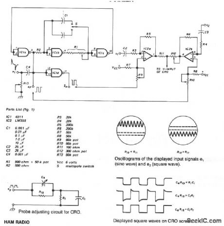
IC1a, IC1b, and IC1c of the quad two-input NAND gate 4011 are connected as an astable multivibrator; IC1d is connected as an inverter. Terminals 3 and 11 of the 4011 produce square waves wit opposite phases. The square waves, ep, at the output of IC1a, passing through differentiator C4R13, then form positive and negative pulses, et. The dual op amps of the LM358 ar, used as two gated amplifiers for singles e1and e2 and fed through terminals 2 and 6, to be displayed simultaneously on the CRO screen.
The two opposite-phase square waves ep, and ep are used to gate IC2a and IC2b at terminals 3 and 5 of the LM358, respectively. Resistances R9 and R10 are preadjusted so that one op amp is driven to saturation while the other works normally as an amplifier. Thus, they will amplify signals e1 and e2 alternately, and two separate traces will be displayed on the screen. Resistance R12 can be varied to adjust the vertical separation of the two traces.
Select a suitable value for C1 with switch S, and adjust the pot of R1. The frequency of square waves can be varied from 1 to 106 cps. This process is necessary for stabilizing the waveforms dtsptiyed on the screen. A common supply of 6 V is used in the circuit.
(View)
View full Circuit Diagram | Comments | Reading(1385)
OSCILLOSCOPE_TRIGGERED_SWEEP
Published:2009/7/9 2:05:00 Author:May
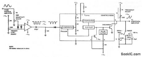
The circuit's input op amp triggers the timer, sets its flip-flop and cuts off its discharge transistor so that capacitor C can charge. When capacitor voltage reaches the timer's control voltage of 0.33 VCC the flip-flop resets and the transistor conducts, discharging the capacitor. Greater linearity can be achieved by substituting a constant-current source for frequency adjust resistor R. (View)
View full Circuit Diagram | Comments | Reading(631)
CHROMA_DEMODULATOR_WITH_RGB_MATRIX
Published:2009/7/9 2:04:00 Author:May
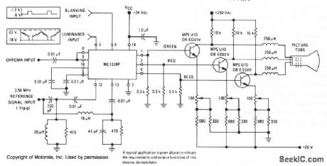
The MC1324 provides chroma demodulation recovering recooling the R, G, and B signals to drive video amps for each color difference signal. The luminance signal and chrominance signal are matrixed to get the R. G. and B signals. (View)
View full Circuit Diagram | Comments | Reading(758)
PULSE_WIDTH_MODULATOR
Published:2009/7/9 2:03:00 Author:May
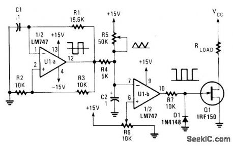


This circuit allows the effective power in a load to be controlled by varying the duty cycle of the on/off ratio of load current. No power is dissipated in the switching circuit.U1A generates a bipolar square wave that is integrated into a triangle by R4 and C2. Reference Voltage from R6 is fed to a comparator. The triangle ware on C2 goes to the comparator as well. By varying the reference voltage (R6), the output waveform is a variable width pulse, that drives Q1. R6 controls on/off ratio and therefore load power. R5 sets the offset of the triangle wzcve across C2. (View)
View full Circuit Diagram | Comments | Reading(0)
VOICE_SCRAMBLER_DISGUISER_CIRCUIT
Published:2009/7/9 2:01:00 Author:May
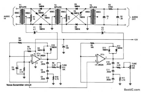
This circuit uses two balanced modulators to produce a DSB signal and then reinsert the carrier, except the carrier now has a different frequency. This causes an input signal to be distorted. A voice signal will be recognizable with this circuit, but the original speakers' voice will not be identiftable with correct adjustments.
Two LM324 op amps act as oscillators that are tuneable from 2 to 3.5 kHz. The frequencies are set with R12 and R13. T1, T2, and T3 are 600Ω CT/600Ω audio transformers-available from Mouser Elec-tronics, Inc. (View)
View full Circuit Diagram | Comments | Reading(1259)
SINGLE_SUPPLY_WIDE_RANGE_SYNC_SEPARATOR
Published:2009/7/9 2:01:00 Author:May
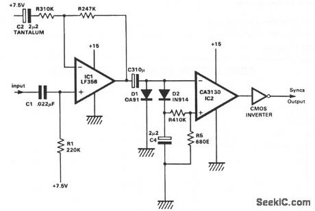
This circuit extracts the sync pulses from a video signal over a wide range of amplitudes and operates a single +15 V supply. IC1 buffers and amplifies the incoming signal and applies it via C3 to the peak detector, consisting of D2 and C4. It is also applied to one input of a comparator, IC2. The other input of IC2 is set at a voltage corresponding to about 0.065 of the peak video amplitude, by the divider R4/R5. The trigger points of IC2 are set near the bottom of the sync pulses which help prevent spurious noise.These resistors also leak across C4, so they must be chosen as a compromise between excessive ripple and speed of response to falling signal levels. The IC2 output swings between O and 15 V and is conve-niently CMOS compatible, but further buffering is advisable, hence the CM0S inverter. Maximum input amplitude is set by saturating IC1's output. The minimum acceptable level is set by the forward voltage drop of the dc restoring clamp D1, which should be either a germanium (as shown) or a Schottky diode. (View)
View full Circuit Diagram | Comments | Reading(700)
OUTPUT_STAGE_POWER_BOOSTER
Published:2009/7/9 1:58:00 Author:May
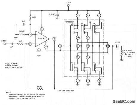
This circuit easily supplements the current-sourcing and current-sinking capability of the CA3130 BiMOS op amp. This arrangement boosts the current-handling capability of the CA3130 output stage by about 2.5 times. (View)
View full Circuit Diagram | Comments | Reading(1093)
PRECISION_HQLF_WAVE_RECTIFIER
Published:2009/7/9 1:58:00 Author:May
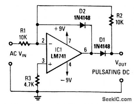
An ac input voltage will cause an output that is a half-wave rectifted version of the input voltage.
(View)
View full Circuit Diagram | Comments | Reading(717)
VOICE_SCRAMBLER_DESCRAMBLER
Published:2009/7/9 1:55:00 Author:May
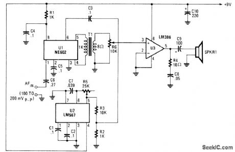
This circuit uses an NE602 as an inversion mixer. U2 is set to run at about 2.5 to 3.5 kHz. U3 drives a loudspeaker. Because speech inversion scrambling is its own inverse, the circuit will also descramble. (View)
View full Circuit Diagram | Comments | Reading(2390)
ELECTRONIC_PHOTOFLASH
Published:2009/7/9 1:55:00 Author:May
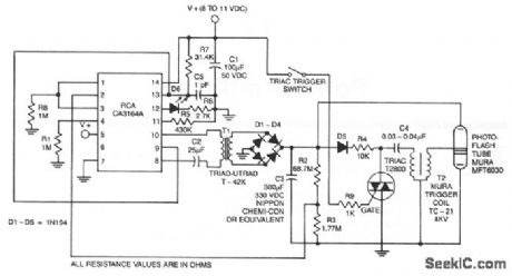
Using the CA3164A BiMOS control chip consumes less than 15 μA during standby, yet it can provide 100 mA of chopped current to the dc-to-dc converter during the energy-reservoir charging cycle. The CA3164A drives the primary of T1 with symmetrically chopped current at a 400 to 2000 Hz rate. The CA3164A's chopper frequency is about 500 Hz; the duty cycle, 50% when R7 is 3.1 4 KΩ. (View)
View full Circuit Diagram | Comments | Reading(720)
SCOPE_EXTENDER
Published:2009/7/9 1:54:00 Author:May
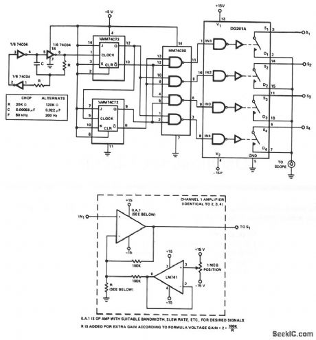
The adapter allows four inputs to be displayed simultaneously on a single trace scope. For low-frequency signals, less than 500 Hz, the adapter is used in the chop mode at a frequency of 50 kHz. The clock can be run faster, but switching glitches and the actual switching time of the DG201A limit the maximum frequency to 200 kHz. High frequencies are best viewed in the alternate mode, with a clock frequency of 200 Hz. When the clock is below 100 Hz, trace flicker becomes objectionable. One of the four inputs is used to trigger the horizontal trace of the scope.
(View)
View full Circuit Diagram | Comments | Reading(672)
XENON_FLASHER
Published:2009/7/9 1:52:00 Author:May
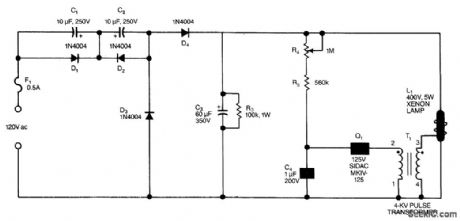
Using a voltage-doubler supply, this circuit charges a 60-μF capacitor and discharges it through a Xenon lamp. The SIDAC device is manufactured by Motorola. It is a two-terminal device that breaks over at a specified voltage. R4, R5, and C4 determine the flash rate. (View)
View full Circuit Diagram | Comments | Reading(2730)
PSEUDORANDOM_SIMULATED_FLICKER_SEQUENCER
Published:2009/7/9 1:48:00 Author:May
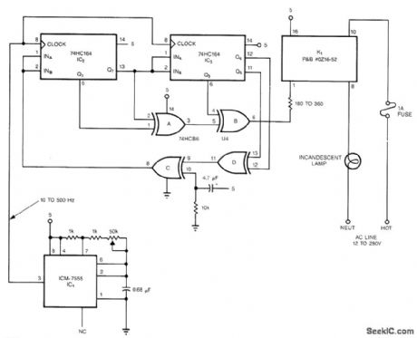
The pseudorandom sequencer drives a solid-state relay, If you power a low-wattage lamp from the relay, the lamp will appear to flicker like a candle’s flame in the wind; using higher-wattage lamps allows you to simulate the blaze of a fireplace or campfire. You can enhance the effect by using three or more such circuits to power an array of lamps. The circuit comprises an oscillator, IC1, and a 15-stage, pseudorandom sequencer, IC2-4. The sequencer produces a serial bit stream that repeats only every 32767 bits. Feedback from the sequenc-er’s stages 14 and 15 go through IC4D and back to the serial input of IC2. Notice the RC network that feeds IC4C; the network feeds a positive pulse into the sequencer to ensure that it won’t get stuck with all zeros at power-up. The leftover XOR gates IC4A and IC4B further scramble the pattern. The serial stream from IC4B drives a solid-state relay that features zero-voltage switching and can handle loads as high as 1A at 12 to 280 Vac. (View)
View full Circuit Diagram | Comments | Reading(803)
DERIVED_CENTER_CHANNEL_STEREO_SYSTEM
Published:2009/7/9 1:48:00 Author:May
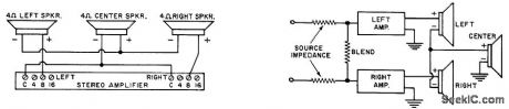
A simple method of deriving a center or third channel without the use of an extra transformer or amplifter. (a) 4-Ω speakers are connected to 8-Ω amplifier taps. 8 and 16-Ω speakers connect to 16-Ω taps. (b) By blending the inputs it is possible to cancel out undesired crosstalk. (View)
View full Circuit Diagram | Comments | Reading(1031)
SLAVE_PHOTOGRAPHIC_XENON_FLASH_TRIGGER
Published:2009/7/9 1:48:00 Author:May


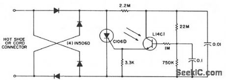
This circuit is used for remote photographic flash units that flash at the same time as the flash attached to the camera. This circuit is designed to the trigger cord or hot shoe connection of a commercial portable flash unit and triggers the unit from the light produced by the light of the flash unit attached to the camera. This provides remote operation without the need for wires or cables between the various units. The flash trigger unit should be connected to the slave flash before turning the flash on to prevent a dV/dt triggered flash on connection. The L14C1 phototransistor has a wide, almost cosine viewing angle, so alignment is not critical. If a very sensitive, more directional remote trigger unit is desired, the circuit can be modified using an L14G2 lensed phototransistor as the sensor.The lens on this transistor provides a viewing angle of approximately 10° and gives over a 10 to 1 improvement in light sensitivity (3 to 1 range improvement). Note that the phototransistor is connected in a self-biasing circuit which is relatively insensitive to slow-changing ambient light, and yet discharges the 0.01-μF capacitor into the C106D gate when illuminated by a photo flash. For a physically smaller size, the C106D can be replaced by a C205D, if the duty cycle is reduced appropriately. (View)
View full Circuit Diagram | Comments | Reading(1159)
TWO_SALLEN_KEY_LOW_PASS_ACTIVE_FILTERS
Published:2009/7/9 1:43:00 Author:May
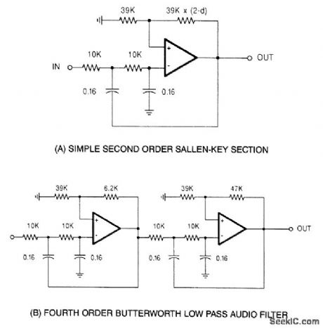
These filters are designed for 10-kΩ impedance level and 1-kHz cutoff frequency, but the components can be scaled as required for other impedances and cutoff frequencies. (View)
View full Circuit Diagram | Comments | Reading(937)
VIDEO_GAIN_BLOCK
Published:2009/7/9 1:41:00 Author:May
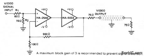
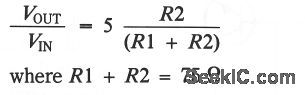
This configuration utilizes the wide bandwidth and speed of HA-2540, plus the output capability of HA-5033. Stabilization circuitry is avoided by operating HA-2540 at a closed loop gain of 10, while maintaining an overall block gain of unity. However, gain of the block can be varied using the equation:A maxlmum block gam of 3is recommended to prevent signal distortinThis ciruit was tested for differential phase and differential gatn using a Tektronix 520A vector scopeand a Tektronix 146 video signal generator Both differential phase and differential gain were too small tobe measured. (View)
View full Circuit Diagram | Comments | Reading(657)
1000_1_TUNING_VOLTAGE_VOLTAGE_CONTROLLED_FILTER
Published:2009/7/9 1:39:00 Author:May
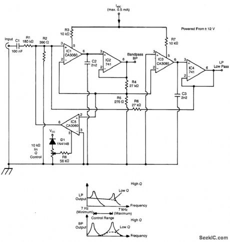
A standard dual integrator ftlter can be constructed using a few CA3080s. By varying IABC, the reso-nant frequency can be swept over a 1000:1 range. At IC1, three are current-controlled integrators. At IC2, four are voltage followers that serve to buffer the high-impedance outputs of the integrators. A third CA3080 (IC5) is used to control the Q factor of the filter. The resonant frequency of the ftlter is linearly proportional to IABC. Hence, this unit is very useful in producing electronic music. Two outputs are pro-duced: a low-pass and a bandpass response. (View)
View full Circuit Diagram | Comments | Reading(820)
CAMERA_ALARM_TRIGGER
Published:2009/7/9 1:36:00 Author:May
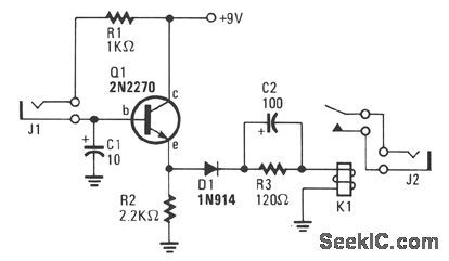
Transistor Q1 remains off until the magnetic switch connected to J1 closes. When that happens, the 9 V is connected through R1 to Q1'S base. Q1 turns on, thereby charging C2 through relay K1, which causes K1's contacts to close. Since the contacts connect via J2 to the remote control jack in the camera, which in turn connects to the camera's shutter release, the closure of K1's contacts will cause the camera's shutter to trigger. After C2 charges, K1 opens because current through its coil ceases; the camera won't take another picture. If Q1 turns off because the magnetic switch on the window or gate opens, C2 discharges and the circuit is ready for another cycle. As long as Q1 remains on, C2 stays charged and prevents K1 from triggering more photos. Capacitor C1 bypasses spurious magnetic switch noises from physical phenomena, such as a rattling window or a gate shaking in the wind, thus reducing the likelihood of an unwanted picture. Resistor R2 biases Q1 and dampens K1/C2 oscillations which might cause contact bounce. Diode D1 prevents C2 from discharging through K1; the relay coil isn't polarity conscious and C2 discharging through it would trigger an unwanted picture. (View)
View full Circuit Diagram | Comments | Reading(665)
SIMPLE_RUMBLE_FILTER
Published:2009/7/9 1:35:00 Author:May
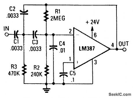
This circuit is a two-section active HP filter using an LM387, with a cutoff below 50 Hz at 12-dB per octave. It will help reduce rumble as a result of turntable defects in record systems. (View)
View full Circuit Diagram | Comments | Reading(851)
| Pages:227/471 At 20221222223224225226227228229230231232233234235236237238239240Under 20 |
Circuit Categories
power supply circuit
Amplifier Circuit
Basic Circuit
LED and Light Circuit
Sensor Circuit
Signal Processing
Electrical Equipment Circuit
Control Circuit
Remote Control Circuit
A/D-D/A Converter Circuit
Audio Circuit
Measuring and Test Circuit
Communication Circuit
Computer-Related Circuit
555 Circuit
Automotive Circuit
Repairing Circuit