
Index 228
ANALOG_DELAY_LINEECHO_AND_REVERB
Published:2009/7/9 1:35:00 Author:May
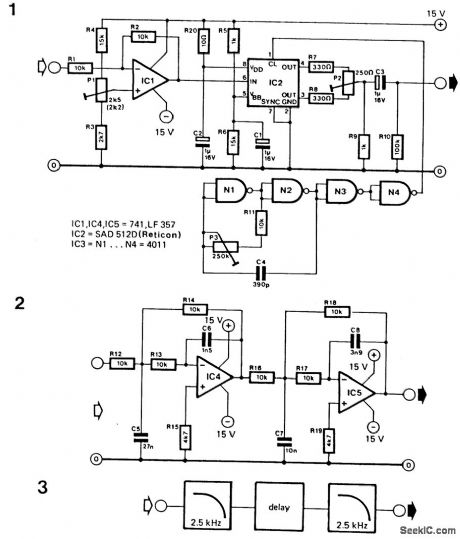
This circuit uses an SAD 512D (Reticon) chip, which is a 512-stage analog shift register. By varying the clock frequency between 5 and 50 kHz, delay time can be set between 51.2 and 5.12 ms. The clock fre-quency must be at least twice the highest audio frequency. (View)
View full Circuit Diagram | Comments | Reading(1689)
Digital programmable voltage reference circuit diagram with 0 ~ 9.99V Output voltage
Published:2011/5/10 4:21:00 Author:Rebekka | Keyword: Digital programmable voltage reference, 0 ~ 9.99V output voltage
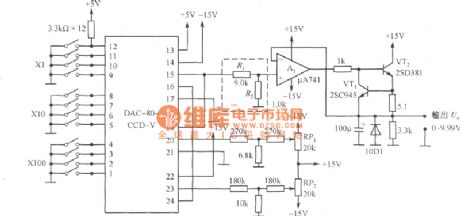
Figure shows the output voltage 0 ~ 9.99V digital programmable reference voltage source circuit. The circuit is composed of 12-bit D / A converter, DAC-80-CCD-V, VT1, VT2, the current amplifier and other components. The larger output current is, the more widespread use it will hace. But it is used for experiment and adjustment of the reference voltage source. The output current is 100mA. If the step voltage is set to be 1mV, you need to add an attenuator composed of the resistance Rl and R2. The output voltage is 0 ~ 9.99V. In Circuit, RPl is used for full-scale adjustment, RP2 is used for zero.
(View)
View full Circuit Diagram | Comments | Reading(2009)
TWO_DOOR_ANNUNCIATOR
Published:2009/7/8 23:06:00 Author:May
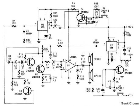
When the pushbuttons at either door are depressed, this circuit generates a different tone for each door. Tones are generated by phase-shift oscillator Q1/Q2. Q3 provides tone frequency change by chang-ing the phase-shift network. U2 and U3 are timers for the tones and Q4/Q5 interface the timers with the pushbuttons. (View)
View full Circuit Diagram | Comments | Reading(829)
TREMOLO
Published:2009/7/8 23:05:00 Author:May
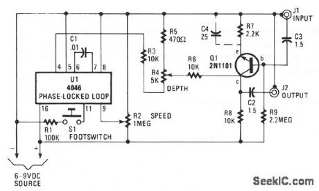
The VCO of U1, a phased-locked loop, produces a low-frequency square-wave signal from 5 Hz to 2500 Hz, which is controlled by varying the voltage to pin 9 via R2. The frequency threshold is set by R1 and C1. Increasing the value of R1 increases the frequency, and decreasing the value of C1 decreases the threshold frequency. Transistor Q1 is operated as an amplifier with the Q point at 4 V, using a transistor with a voltage gain (beta) of 100. The gain without tremolo is about 2 V. With bypass capacitor C4 in the circuit, the gain is set at 33 dB. The instrument drive cannot be greater than 30 mV with C4 in the circuit (no tremolo), to avoid distortion. Without C4, the drive can be 1.5 V maximum with no distortion. U1's output is coupled to the collector of transistor Q1 via depth control R4. The square-wave signal pulls the audio at a frequency determined by R2. The oscillator is activated by foot switch S1. (View)
View full Circuit Diagram | Comments | Reading(1157)
ELECTRONIC_BELL
Published:2009/7/8 23:02:00 Author:May
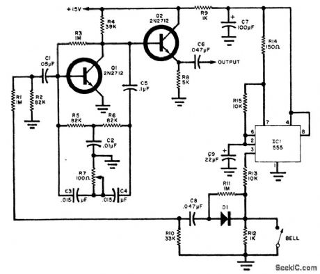
A 555 timer pulses twin-T oscillator Q1.Q2 acts as an output buffer.R7 adjusts the frequency of oscillator Q1. (View)
View full Circuit Diagram | Comments | Reading(0)
SCR_CIRCUIT_WITH_SELF_NTERRUPTING_LOAD
Published:2009/7/8 23:00:00 Author:May
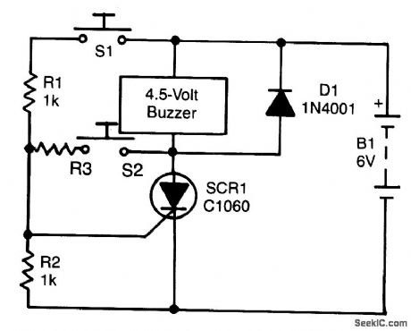
A self-interrupting device connected to a volt-age source functions as a switch that repeatedly opens and closes; therefore, the circuit does not latch in the normal way, so the alarm operates only as long as S1 is closed. Because of the inductive nature of that type of load, a damping diode (D1) must be wired across it.
The circuit can be modified to provide a self-latching action simply by wiring a 470-Ω resistor in parallel with the alarm. The circuit latches because the anode current of the SCR does not fall to zero when the alarm self-interrupts, but to a value that is determined by the value of the R3. The circuit can be unlatched by pressing S2, thereby enabling the anode current to fall to zero when the alarm self-interrupts. (View)
View full Circuit Diagram | Comments | Reading(1161)
WIRELESS_FM_MICROPHONE_2
Published:2009/7/8 23:00:00 Author:May
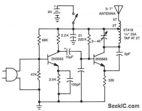
Use standard rf wiring precautions.The best speech clarity is obtained by using an electret microphone. For music reproduction,substitute a dynamic mike element. (View)
View full Circuit Diagram | Comments | Reading(633)
SIMPLE_JFET_PRESELECTOR
Published:2009/7/9 1:14:00 Author:May
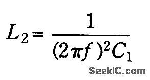
This preselector will improve the performance of simple shortwave receivers. L2 is tuned with Q1.The inductance of L2 is:and L1is found around the cold end of L2. Typically, L1 has 10%of the turnsin L2, or one turn, which-everis larger. (View)
View full Circuit Diagram | Comments | Reading(1006)
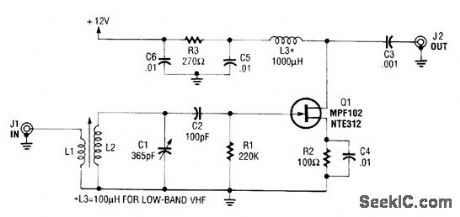
DOUBLE_TUNED_JFET_PRESELECTOR
Published:2009/7/9 1:10:00 Author:May
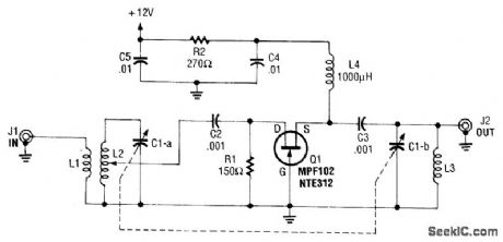
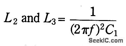
This circuit uses an MPF102 JFET and a double-tuned common-gate amplifier. Gain is typically 10 to 15 dB∶L1≈ 10% turns on L2 or 1 turn (larger of these two). (View)
View full Circuit Diagram | Comments | Reading(2659)
OPTOISOLATOR
Published:2009/7/9 0:54:00 Author:May
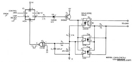
The circuit protects a solid-state relay from overloads. The circuit limits current, automatically discon-nects the load after detecting a short circuit, and develops a fault-condition output signal.In normal operation, the controlling ptP sets the flip-flop, IC1, which turns on transistor Q1. When Q1 turns on, current flows through the solid-state relay's input, thus activating the relay.If an overcurrent or fault condition occurs, the excessive load current flowing through the relay develops enough potential across sense resistor R5 to turn on one of the optoisolators, IC4A or IC4B. The optoisolator's output transistor diverts current around the solid-state relay's input, which limits the cur-rent that the relay's output can pass.If the overload is severe enough, the optoisolator pulls the input of the Schmitt trigger above its threshold, thus clearing the flip-flop and turning off the solid-state relay. R2 has two functions: It keeps the input of the Schmitt trigger below 5 V max. to prevent latchup, and it forms an RC filter in conjunction with C1. The RC filter prevents spurious triggering of the Schmitt trigger. You can use the output of the flip-flop to signal overload conditions to the controlling μP. (View)
View full Circuit Diagram | Comments | Reading(2299)
120_KHz_500_W_INDUCTION_HEATER
Published:2009/7/9 0:52:00 Author:May
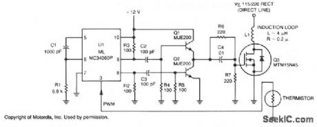
Variable width pulses with fast rise times are provided by U1, and MC34060 operating at 120 kHz, the optimum frequency for heating aluminum alloy containers. The pulse width is modulated by sensing the temperature of the target with a thermistor, using its negative temperature coefficient to change pulse duration. The MC34060 produces output pulses that are accoupled to push-pull MJE200 transistors Q1 and Q2. This IC provides the current needed to ensure fast switching for MTM15N45 TMOS power FET Q3.The estimated efficiency is 80%, based on switching losses and an RON of 0.4 Ω (max). The MTM15N45, with maximum ratings of 15 A and 450 V, was chosen because the induction heater might be operated from either 115 or 220 V sources. A modest heatsink is required because 100 W is dissipated in the power FETs at a full output power of 500 W. (View)
View full Circuit Diagram | Comments | Reading(6338)
FOURTH_ORDER_100_Hz_HIGH_PASS_FILTER
Published:2009/7/9 0:05:00 Author:May
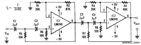
This filter, using two sections of LM741, can be scaled in frequency ,If desired. (View)
View full Circuit Diagram | Comments | Reading(1207)
300_TO_3400Hz_SECOND_ORDER_SPEECH_FILTER
Published:2009/7/9 0:03:00 Author:May

Using two op amps,this filter is designed for second-order response.It has a bandpass of 300 to 3 400Hz,for applications In speech or telephone work. (View)
View full Circuit Diagram | Comments | Reading(2276)
VOCAL_ELIMINATOR
Published:2009/7/9 0:02:00 Author:May
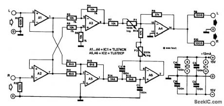
Otherwise properly mixed sounds often suffer from a predominant solo voice (which might, of course, be the intention). If such a voice needs to be suppressed, the present circuit will do the job admirably.
The circuit is based on the fact that solo voices are invariably situated at the center of the stereo recordings that are to be mixed. Thus, voice levels in the left-and right-hand channels are about equal. Arithmetically, therefore, left minus right equals zero; that is, a mono signal without voice.
There is, however, a problem: the sound levels of bass instruments, more particularly the double basses, are also just about the same in the two channels. On the one hand low-frequency sounds are virtu-ally nondirectional and on the other hand, the recording engineers purposely use these frequencies to give a balance between the two channels.
However, the bass instruments can be recovered by adding those appearing in the left+right signal to the left-right signal. The whole procedure is easily followed in the circuit diagram. The incoming stereo signal is buffered by Al and A2. The buffered signal is then fed to differential amplifier A3 and subse-quently to summing amplifier A5. The latter is followed by a low-pass filter formed by A6. You can choose between a first-order and a second-order filter by respectively omitting or fitting C2. Listen to what sounds best.
The low-frequency signal and the difference signal are applied to summing amplifier A4. The balance between the two is set by P1 and P2 to individual taste.
You have noticed that the circuit does not contain input or output capacitors. If you wish, output capac-itors can be added without detriment. However, adding input capacitors is not advisable, because the con-sequent phase shift would adversely affect the circuit operation. (View)
View full Circuit Diagram | Comments | Reading(1584)
LOW_FTEQUENCY_MULTIPLIER
Published:2009/7/9 0:01:00 Author:May
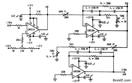


This circuit uses a comparator as a Schmitt trigger (311H) and two active bandpass filters LM318H).3-kHz output is obtained. Higher harmonics (preferably odd) can be obtained by tuning the active filters to the desired frequency.N can be 1, 3, 5, 7, 9, etc. Even harmonics can be produced by substituting a full-wave rectifier or absolute-value circuit for the Schmitt-trigger comparator. (View)
View full Circuit Diagram | Comments | Reading(1113)
TWO_SECTION_300_3000Hz_SPEECH_FILTER
Published:2009/7/9 0:01:00 Author:May
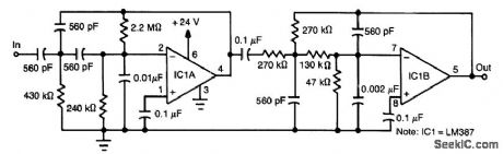
An LM387 dual low-noise amplifier is used in an active filter. Both sections are used to produce second-order HP and LP filters, respectively. (View)
View full Circuit Diagram | Comments | Reading(1687)
ANTIALASING_AND_SYNC_COMPENSATION_FILTER
Published:2009/7/8 23:58:00 Author:May
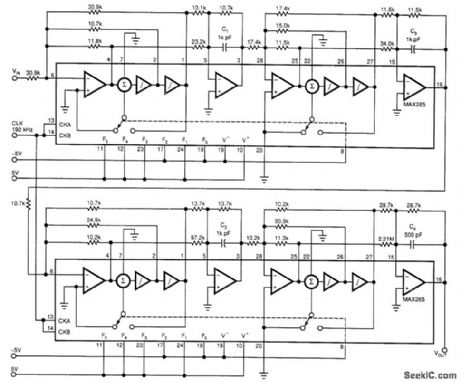
Two dual-biquad filter ciUps and some external components form a multipurpose filter to reconstruct D/A converter signals. Connected to a converter’s output, the filter provides antialiasing, reduces the D/A converter’s quantization noise, and compensates for sin(πx) ÷ (πx)-the sync function (attenuation).
The circuit incorporates an inverse-sync function that operates to one-third of the converter’s sample rate. Beyond one-third, the filter’s response shifts to a stopband filter, which provides -70 dB attenua-tion. This attenuation conforms to the converter’s inherent signal-to-noise ratio and quantization error.
To prevent aliasing, the stopband edge must be no higher than the Nyquist frequency (fsn÷2). To achieve 70-dB stopband rejection with this eighth-order filter requires a transition ratio (fSTOPgAND÷fPASSsAND) of 1.5, which sets the passband’s upper limit at fS÷3.
Notice also that you can apply a simple divide-by-64 circuit to the 192-kHz clock frequency to set the necessary 3× ratio between the converter’s sample rate and the filter’s 1-kHz comer frequency. The V+, V-, and the FO through F5 connections program each filter chip for an fCLK/f0 ratio of 191.64. (View)
View full Circuit Diagram | Comments | Reading(893)
GASFET_FREQUENCY_DOUBLER
Published:2009/7/8 23:53:00 Author:May

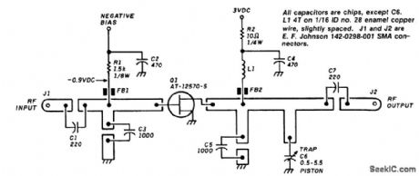
This circuit will produce over + 10 dBm in the 1 800-3000-MHz range. Drive power is 7 dBm in the 900-to-1500-MHz range. The PC board is G-10 Epoxy doublesided. Artwork is shown above, as well as parts placement connectors suitable for these frequencies (such as SMA) should be used. A negative bias supply of 0 to 3 V is required. (View)
View full Circuit Diagram | Comments | Reading(719)
9_V_FROM_12_V
Published:2009/7/8 23:51:00 Author:May
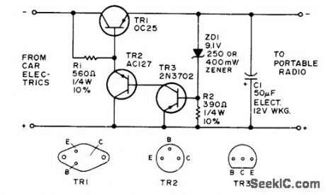
Developed for economical operation of 9-V portable radio from 12-V storage battery of car-Circuits' 73 Magazine,Marche 1975.p 136 (View)
View full Circuit Diagram | Comments | Reading(572)
JFET_SERIES_PASS
Published:2009/7/8 23:50:00 Author:May
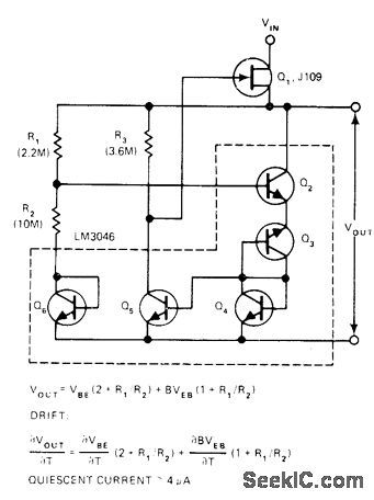
Use of JFET as series-pass element for LM3046 voltage regulator IC minimlzes battery drain In microprocessor systemapplications Pass element needs no preregu-lation because drive comes from reguiated output Gate source is isolated from line by drainand thus provides excellent line regulation.-J.Maxwell、Voltage Regulator Bridges Gap Between IC's and Zeners‘EDNMagazine.Sept 5、1977、p 178-179 (View)
View full Circuit Diagram | Comments | Reading(1140)
| Pages:228/471 At 20221222223224225226227228229230231232233234235236237238239240Under 20 |
Circuit Categories
power supply circuit
Amplifier Circuit
Basic Circuit
LED and Light Circuit
Sensor Circuit
Signal Processing
Electrical Equipment Circuit
Control Circuit
Remote Control Circuit
A/D-D/A Converter Circuit
Audio Circuit
Measuring and Test Circuit
Communication Circuit
Computer-Related Circuit
555 Circuit
Automotive Circuit
Repairing Circuit