
Index 236
T_ATTENUATOR_
Published:2009/7/8 4:22:00 Author:May
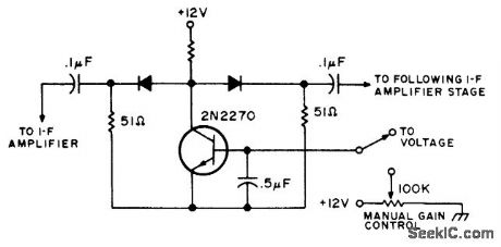
When inserted between stages of IF amplifier, circuit acts as three.section attenuator with dynamic range greater than 60 dB. Can be controlled by positive voltage from AVC system of receiver or manually with 100K pot. Use PIN diodes.-Super Circuits, 73 Magazine, Aug. 1975, p 140. (View)
View full Circuit Diagram | Comments | Reading(940)
TRACK_AND_HOLD
Published:2009/7/8 4:22:00 Author:May
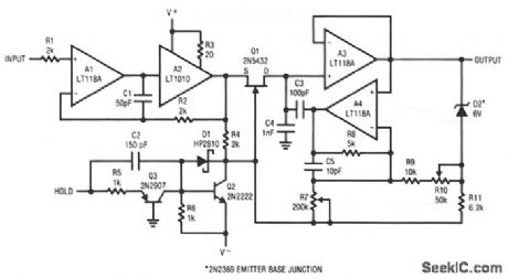
The 5-MHz track and hold shown here has a 400-kHz power bandwidth driving ±10 V. A buffered input follower drives the hold capacitor, C4, through Q1, a low resistance FET switch. The positive hold command is supplied by TTL logic, with Q3 level shifting to the switch driver, Q2. The output is buffered by A3. When the gate is driven to V- for hold, it pulls the charge out of the hold capacitor. A cornpensating charge is put into the hold capacitor through C3. The step into hold is made independent of the input level with R7, and adjusted to zero with R10.Since internal dissipation can be quite high when driving fast signals into a capacitive load, using a buffer in a power package is recommended. Raising the buffer quiescent current to 40 mA with R3 improves frequency response. (View)
View full Circuit Diagram | Comments | Reading(1292)
50-MHz_TRIGGER
Published:2009/7/8 4:20:00 Author:May
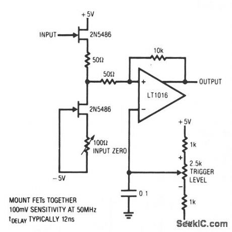
This has a stable trigger 100 mV sensitivity at 50 MHz. The FETs comprise a simple high-speed buffer and the LT1016 compares the buffer's out-put to the potential at the trigger level potentiometer, which can be of either polarity. The 10-KΩ resistor provides hysteresis, eliminating chattering caused by noisy input signals. To calibrate this circuit, ground the input and adjust the input zero control for 0 V at Q2's drain terminal. (View)
View full Circuit Diagram | Comments | Reading(649)
IF_WITH_NOISE_BLANKER
Published:2009/7/8 4:19:00 Author:May
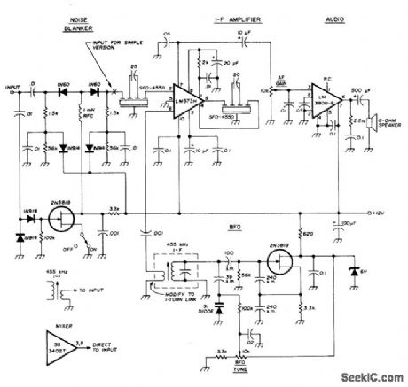
Addition of BFO andnoise blankerto 455-kHzIF amplifier gives setupfor testing new tuners and front ends Two methods of coupling into ampliier are shown.LM373H IC with two Murata SFD-455D ceramic filters fulfills requirements for IF amρlifer,delector,and AGC functions.-R.Megirian,Design Ideas for Miniature Communications Receivers,Ham Radio,April 1976,p 18-25. (View)
View full Circuit Diagram | Comments | Reading(2566)
BAR_CODE_SCANNER
Published:2009/7/8 4:19:00 Author:May
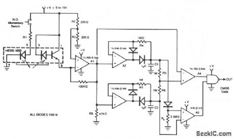
The circuit illustrates a method of interfacing a HEDS-1000 emitter-detector pair with a HA-5144 for use as a bar-code scanner circuit. The HA-5144 is used as an amplifier system which converts the bar and space widths of the printed bar code into a pulse-width modulated digitA1 signal. Amplifier A1 is used to amplify the current output of the detector. The output of A1 is passed to two precision peak-detector circuits which detect the positive and negative peaks of the received signal. Amplifier A4 is used as a comparator whose reference is maintained at the midpoint of the peak-to-peak signA1 by resistors R5 and R6. This provides a more accurate edge detection and less ambiguity in bar width. Amplifier A5 is used as an optionA1 noise gate which only allows data to pass through the gate when the peak-to-peak modulation sign A1 is larger than one diode drop. This circuit is operated by a single supply voltage with low-power consumption which makes it ideal for battery-operated data entry systems. (View)
View full Circuit Diagram | Comments | Reading(3576)
FLAME_IGNITOR
Published:2009/7/8 4:17:00 Author:May
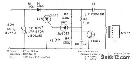
The spark developed by the circuit is suitable for a gas ignitor. Capacitor C1 is charged through R1 and D1 toward peak line voltage. C2 is simultaneously being charged at a slower rate through R5. When the charge on C2 is sufficient to trigger the PUT, the SCR is triggered on, providing a rapid discharge path for C1 through the transformer primary. The SCR is triggered about 20 times per second with the component values shown. The L14G3 serves as a flame sensor. When ignition is achieved and sensed by the photodetector, the low VCE prevents further SCR triggering. (View)
View full Circuit Diagram | Comments | Reading(1005)
POSITIVE_INPUT_NEGATIVE_OUTPUT_OHARGE_PUMP
Published:2009/7/8 4:10:00 Author:May
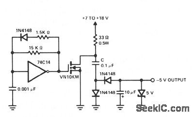
A charge pump is a simple means of generating a low-power voltage supply of opposite polarity from the main supply. The 74C14 IC is a self-oscil-lating driver for the MOSFET power switch. It produces a pulse width of 6.5 prs at a repetition frequency of 100 kHz. When the MOSFET device is off, capacitor C is charged to the positive supply.When the power through the MOSFET switches on, C delivers a negative voltage through the series diode to the output. The zener serves as a dissipative regulator. Because the MOSFET switches fast, operation at high frequencies allows the capacitors in the system to be small. (View)
View full Circuit Diagram | Comments | Reading(880)
ELECTRONIC_MUSIC
Published:2009/7/8 4:09:00 Author:May
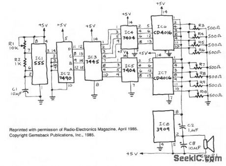
IC1, a 555 timer, is set up as an astable multivibrator to produce the signal that triggers IC2, a 7490 decade counter. That IC, in turn, produces a BCD output that is fed to IC3, a 7445 BCD-to-decimal decoder/driver. IC3's output is inverted by two hex inverters, IC4 and IC5. The outputs of IC4 and IC5 are inputted to control pins on IC6 and IC7, CD4016 CMOS quad bilateral switches. As those switches open and close, different resistances (as set by potentiometers R3 through R10) are inserted into the sound-generating circuit made from IC8. The frequency at the outputs of IC6 and IC7 are adjusted to various rates, using potentiometers R3 through R10, to produce the desired tones. Capacitors can be placed in series with the potentiometers to produce a sloping sound instead of a straight tone. The negative-going output signals of IC6 and IC7 are fed through a common bus to pin 8 of IC8. (View)
View full Circuit Diagram | Comments | Reading(2099)
BUG_TRACER
Published:2009/7/8 4:06:00 Author:May
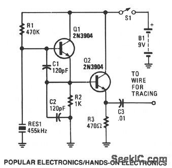
The bug tracer is made up of a simple rf-injector circuit consisting of Q1 and Q2, and a pocketsize, AM broadcast receiver. The two-transistor rf-injector circuit supplies a constant rf signal to one end of a cable. Then the AM receiver is used as a detector, allowing you to trace the wire to its source.
Transistor Q1, along with piezoelectric ceranuc resonator RES1, make up a simple rf oscillator that operates either at or near the AM-radio, 455-kHz, i-f frequency. That means that the second or third harmonic signal can easily be picked up by the receiver. Transistor Q2 is connected to an emitter-follower circuit to protect the oscillator from output loading; that helps to stabilize the output frequency and signal level. (View)
View full Circuit Diagram | Comments | Reading(3089)
28_MHz_LOW_NOISE
Published:2009/7/8 4:05:00 Author:May
Developed for use with 2304-MHz balanced mixer. Provides required match between 50-ohm mixer output and input of 28-MHz IF amplifier in UHF receiver.Input and output connections are made with short lengths of RG-58/U coax. Noise figure is less than 1.5 dB.-L. May and B. Lowe, A Simple and Efficient Mixer for 2304 MHz, QST, April 1974, p 15-19 and 31. (View)
View full Circuit Diagram | Comments | Reading(751)
CENTRAL_IMAGE_CANCELLER
Published:2009/7/8 4:05:00 Author:May

The circuit allows you to eliminate the vocal potion of an audio signal, while leaving the instrumental portion. The circuit mixes two channels that must be 180° out of phase, so the signals that form the center-stereo image is canceled out. Those signals usually appear in phase. Resistor R3 biases the noninverting input of UI from a center tap formed by resistors RI and R4, and capacitor C3. Resistor R4, capacitor C3, and potentiometer R6 form a negative-feedback circuit that establishes the closed-loop voltage gain of UI at unity. The signal is inverted between the input and output. (View)
View full Circuit Diagram | Comments | Reading(603)
TOUCH_SWITCH_2
Published:2009/7/8 4:02:00 Author:May
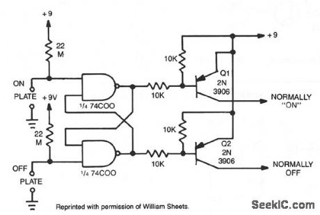
When the plate is touched, the gate input becomes low, changing the state of the latch.Q1 and Q2 give alternate N-on-N-off outputs. (View)
View full Circuit Diagram | Comments | Reading(1460)
IF_FILTER_FOR_CW
Published:2009/7/8 4:00:00 Author:May
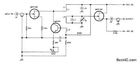
Circuit acts Iike variable filter having adjustable bandwidth, with enough gain to compensate for insertion Ioss in CW receiver. Used to isolate weak CW signals despite noise and interference, as required in lowpower amateur work. FET input is directly coupled to collector of HEP55 serving as Q.multiplier regenerative amplifier. Transformer L1-L3 provides feedback. Filter is connected in serieswith input end of IF strip,following 1.2-kHz mechanical filter. When two CW signals are received, one can be eliminated by adjusting CA to recenter passband of filter. Current drain of 6 mA can be supplied by two 6-V batteries. For 455-kHz IF, C is 470 pF, CA is 7-45 pF, and L1-L2-L3 are 12-115-24 turns No.32 enamel on Amidon T44-15 core.-S. M. Olberg, Vari-Q Filter, Ham Radio, Sept. 1973, p 62-65. (View)
View full Circuit Diagram | Comments | Reading(737)
POSITIVE_TRIGGERED_TOUCH_CIRCUIT
Published:2009/7/8 3:38:00 Author:May
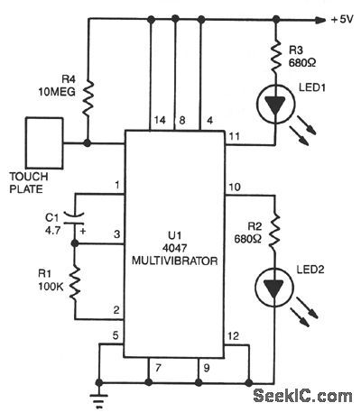
LED1 and LED2 indicators turn on and remain on, each time the circuit is triggered. During the timing cycle, U1's Q output at pin 11 becomes positive when the Q output at pin 11 becomes negative. The two LEDs can be removed and the Q and Q outputs at pins 10 and 11, respectively, can be used to trigger some other circuit. (View)
View full Circuit Diagram | Comments | Reading(687)
455_kHz_CASCODE_IF
Published:2009/7/8 3:35:00 Author:May
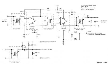
Sections of Signetics NE510A transistor array serve as active elements for IF strip using standard transformers.Voltage gain is 66 dB when gain-control input is grounded. Altemate detector connection for including AGC is shown below.- Signetics Analog Data Manual, Signetics, Sunnyvale, CA, 1977, p 746-747. (View)
View full Circuit Diagram | Comments | Reading(980)
NEGATIVE_TRIGGERED_TOUCH_CIRCUIT
Published:2009/7/8 3:32:00 Author:May
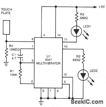
The 4047 is configured as a monostable multivibrator circuit or one shot that is set up to trigger on a negative-transition of the signal applied to its pin 6 input. The multi ibrator's on time is determined by the values of R1 and C1. Although R1 is shown to be a 100-K unit, its value can be anything between 10 K and 1 MΩ . Capacitor C1 can be a nonpolarized capacitor with any practical value above 100 pF. By making R4's value extremely high, the circuit can be used as a touch-triggered one-shot multivibrator. If the value of R4 is reduced to a much lower value, such as 10 KΩ , the circuit can be triggered with a negative pulse through 0.1-μF capacitor connected to pin 6. With a 100-K Ω resistor for R1, and a 4.7-μF electrolytic capacitor for C1, the circuit's on time is about 0.6 second. When R1 is increased to 470 K Ω, the on time of the circuit is increased to over 6 seconds. (View)
View full Circuit Diagram | Comments | Reading(1421)
60_MHz_WITH_80_dB_POWER_GAIN
Published:2009/7/8 3:32:00 Author:May
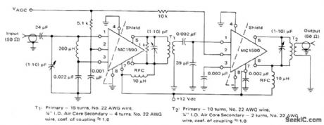
T-stage tuned IF ampIifier achIeves maximum gain and output signal swing capability by using differential-mode coupling for interstage and output network Overall bandwidth is 1.5 MHz Resistors in series with AGC pins 2 of opamp stages provide more efficient AGC action,-B.Trout,''A High Gain Integrated Circuit RF-IF Amplifier with Wide Range AGC.''Motorola,Phoenix,AZ.1975,an-513,p 8. (View)
View full Circuit Diagram | Comments | Reading(659)
001°C_CONTROL_WITH_OPAMP_COMPABA_TOR
Published:2009/7/8 3:27:00 Author:May
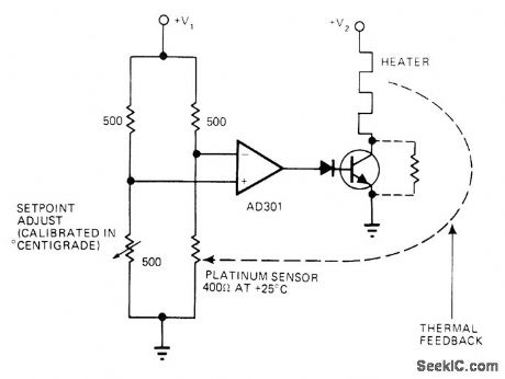
Uses platinum sensor in bridge configuration, with opamp connected across bridge differentially. When cold, sensor resistance is Iess than 500 ohms so opamp saturates to give positive output that tums on power transistor and heater. As oven warms, sensor resistance increases, brklge balance shifts, and heater is cut off.-J. Williams, Designer's Guide to: Temperature Control, EDNMagazine, June 20, 1977, p 87-95.
(View)
View full Circuit Diagram | Comments | Reading(575)
RUMBLE_SCRATCH_FILTER
Published:2009/7/8 3:26:00 Author:May
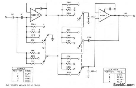
This is a variable bandpass amplifier with adjustable low- and high-frequency cutoffs. (View)
View full Circuit Diagram | Comments | Reading(0)
CRYSTAL_OVEN
Published:2009/7/8 3:26:00 Author:May
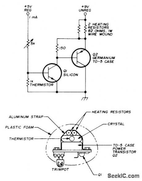
All components for pioportional temperature control circuit are mounted on crystal, so total power of 2 W maximum serves for maintaining crystal temperature.Thermistor is about 1K at room emperature.Transistor types are not critical butshould have low leakage currents. Thermistor current of about 1-mA should be much more than O.1-mA base current of Q1. If Q2 is silicon, increase 150-on resistor to 680 ohms.-P. H. Mathieson, Simple Crystal Oven, Ham Radio, April1976, p 66. (View)
View full Circuit Diagram | Comments | Reading(1280)
| Pages:236/471 At 20221222223224225226227228229230231232233234235236237238239240Under 20 |
Circuit Categories
power supply circuit
Amplifier Circuit
Basic Circuit
LED and Light Circuit
Sensor Circuit
Signal Processing
Electrical Equipment Circuit
Control Circuit
Remote Control Circuit
A/D-D/A Converter Circuit
Audio Circuit
Measuring and Test Circuit
Communication Circuit
Computer-Related Circuit
555 Circuit
Automotive Circuit
Repairing Circuit