
Index 224
FET_BIPOLAR_DARLINGTON
Published:2009/7/9 4:37:00 Author:May
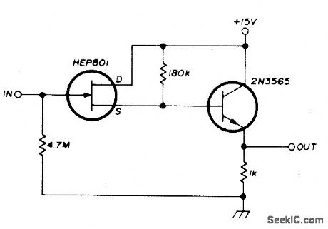
Can be used as meter interface amplifier, impedance transformer, coax driver, or relay actuator. Combination of unipolar and bipolar transistors gives desirable amplifying features of each solid-state device.-I. M. Gottlieb, A New Look at Solid-State Amplifiers, Ham Radio, Feb. 1976, p 16-19. (View)
View full Circuit Diagram | Comments | Reading(1654)
ELECTRONIC_ROULETTE_GAME
Published:2009/7/9 4:36:00 Author:May
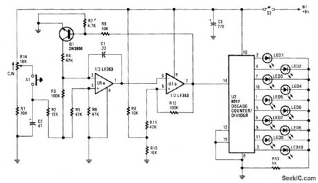
R14 is set for an initial starting speed of the oscillator U1A and U1B. As C2 charges, oscillation begins slowing down as C2 discharges, giving a roulette-wheel effect on LED S1 through 10. The LED that remains on is the winning number. (View)
View full Circuit Diagram | Comments | Reading(1507)
HIGH_VOLTAGE_REGULATOR
Published:2009/7/9 4:34:00 Author:May
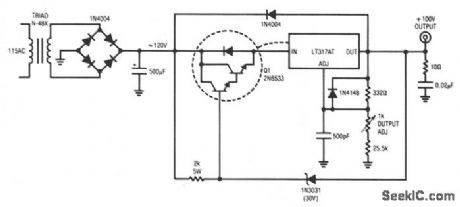
The regulator delivers 100-V at 100 mA and withstands shorts to ground。Even at 100 V output,the LT317A functions in the normal mode,maintainting 1.2 C between its output and adjustment pin.Under these conditions, the 30-V zener is off and Q1 conducts.When an output short occurs, the zener conducts, forcing Q1's base to 30 V. This causes Q1's emitter to clamp 2 VBES below VZ, well VIN-VOUT rating of the regulator.Under these conditions,Q1,a high-voltage device,sustains 90 V- VCE at whatever current the transformer specified saturates at 130 mA,while Q1 safely dissipates 12 W.If Q1 and the LT317A are thermally coupled, the regulator will soon go into thermal shutdown and oscillation will commence,This action will continue, protecting the load and the regulator as long as the output remalns shorted.The 500-pF capacitor and the 10 Ω/0.02 μF damper aid transient response and thediodes provide safe discharge paths for the capacitors. (View)
View full Circuit Diagram | Comments | Reading(1122)
NANOAMMETER
Published:2009/7/9 4:34:00 Author:May
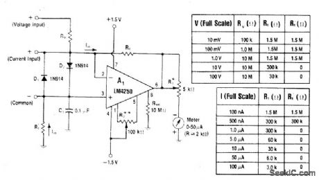
Programmable amplifier operating from ±1.5 V supply such as D cells is used as current-to-voltage convener. Offset null of A1 is used to minimize input offset voltage enor. If programmed for low bias current, amplifier can convert currents as small as 100 nA with less than 1% error,Resistor values for variety of current and voltage ranges are give in tables. Adjust R1 to calibrate meter, and adjust R2 to null input offset voltage on lowest range.Not suitable for higher current ranges because power drain is excessive above 100 μA.-W. G. Jung, IC Op-Amp Cookbook, HowardW Sams, Indianapolis, IN, 1974, p 414-417. (View)
View full Circuit Diagram | Comments | Reading(5187)
CAR_ALARM_WITH_HORN_AS_LOUDSPEAKER
Published:2009/7/9 4:33:00 Author:May
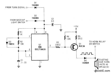
An auto horn will work as a speaker of limited audio-frequency range. This circuit uses a 555 timer as an oscillator to drive an MJE34 transistor, which in turn drives the horn. Normal horn operation is ensured by blocking diode D4. (View)
View full Circuit Diagram | Comments | Reading(881)
3_25_V_DC_DC_CONVERTER
Published:2009/7/9 4:26:00 Author:May
View full Circuit Diagram | Comments | Reading(564)
HIGH_VOLTAGE_INVERTER
Published:2009/7/9 4:25:00 Author:May
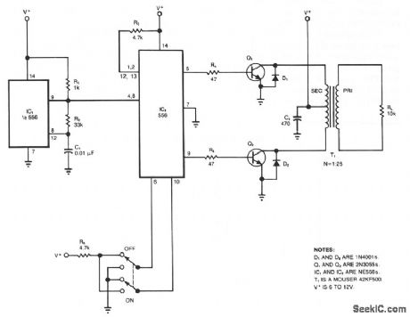
The circuit converts a dc voltage (V+) to a high-amplitude square wave in the audio-frequency range. The dual timer, IC2, provides an inexpensive alternative to the traditional transformer for providing complementary base drive to the power transistors, Q1 and Q2. You can convert a 6 to 12 V battery output, for example, to an ac amplitude, which is limited primarily by the power rating of transformer T1. Connect timer IC1 as an oscillator to provide a symmetrical square-wave drive to both inputs of IC2. The timing components, R2 and C1, produce a 2.2-kHz output frequency. By connecting half of IC2 in the inverting mode and the other half in noninverting mode, the timer's outputs alternately drive the two transistors.You can operate the audio-output transformer, T1, as a step-up transformer by connecting it backwards—using the output winding as an input. The transformer delivers an output voltage across RL of 4 × N × V+V pk-pk, where N is the transformer turns ratio. For the circuit shown, the output swing is 100 × V+V pk-pk. (View)
View full Circuit Diagram | Comments | Reading(1035)
HIGH_EFFICIENCY_FLYBACK_VOLTAGE_CONVERTER
Published:2009/7/9 4:25:00 Author:May
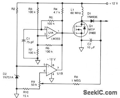
U1 is a dual voltage comparator with open collector outputs. The A side is an oscillator operating at 100 kHz, and the B side is part of the regulation circuit that compares a fraction of the output voltage to a reference generated by zener diode D2.The output of U1A is applied directly to the gate of Q1. During the positive half-cycle of the Q1 gate voltage, energy is stored in L1; in the negative half, the energy is discharged into C2. A portion of the output voltage is fed back to U1B to provide regulation. The output voltage is adjustable by changing feedback potentiometer R9.Using the component values shown will produce a nominal 300-V output from a 12-V source. However, the circuit maximum output voltage is limited by R10; a lower value for R10 yields a higher output voltage. The output voltage is also limited by the breakdown of values Q1, L1, D1, and C2. (View)
View full Circuit Diagram | Comments | Reading(925)
AUTO_TURN_OFF_ALARM_WITH_8_MINUTE_DELAY
Published:2009/7/9 4:24:00 Author:May
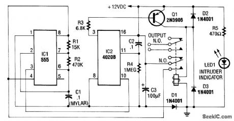
This circuit uses a NE555 timer and CD4020B. When + 12 Vdc is applied to the circuit, the output of IC2 is set low via C2, which turns on the relay, and IC1, a pulse generator. IC1 pulses counter IC2. After 8192 clocks, IC2 output (pin 3) goes high, cuts off Q2, and completes the cycle. (View)
View full Circuit Diagram | Comments | Reading(558)
LIGHT_METER_WITH_LED_READOUT
Published:2009/7/9 4:23:00 Author:May
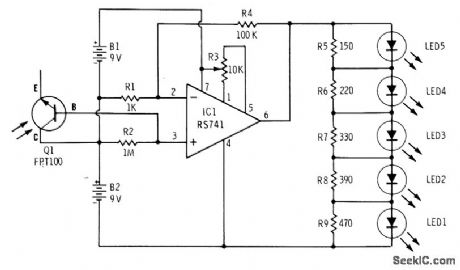
Light onphototransistorQ1 (Radio Shack 276-130) produces voltage change across R2 for amplification by opamp whose output drives array fiveLEDs forming bar graph voltage indicator. Adjust R3 initially for highest sensitivity by tuming off room lights and rotating until LED 1 just stops glowing. Now, as light is gradually increased on sensor, LEDs come on one by one in upward sequence and stay on until all five are lit. Solar cells or selenium cells can be used in place of phototransistor.-F. M. Mims, Opto-electronic Projects, Vol. 1, Radio Shack, Fort Worth, TX, 1977, 2nd Ed., p 85-93. (View)
View full Circuit Diagram | Comments | Reading(1427)
BACKUP_BEEPER
Published:2009/7/9 4:22:00 Author:May
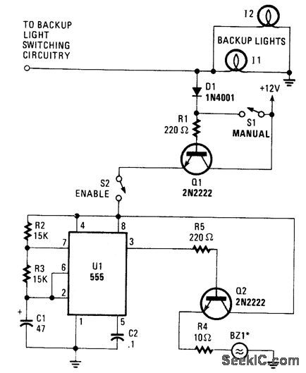
When the vehicle's backup lights kick on, or when the manual switch (S1) is closed, a small current is fed to the base of Q1. Transistor Q1 allows current to flow through it and, if the enable switch (S2) is closed, it sends 12 V to UI, a 555 timer. Timer UI sends high pulses that last 0.97713 s and low signals that last 0.488565 s to the base of Q2. When UI switches Q2 on, it sends 12 V to BZ1, a piezoelectric buzzer. For best results, the buzzer should be mounted under the vehicle-somewhere where people around the car can hear the warning beeps. (View)
View full Circuit Diagram | Comments | Reading(794)
EFFICIENT_SUPPLY_SPLITTER
Published:2009/7/9 4:20:00 Author:May
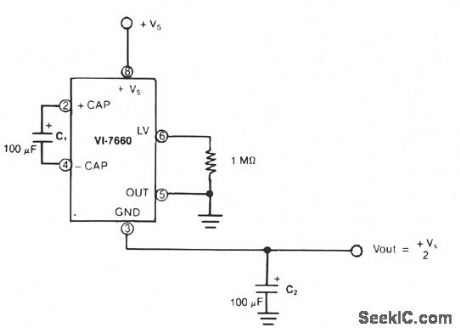
In this application, the VI-7660 is connected as a voltage splitter. Note that the normal output pin is connected to ground and the normal ground pin is used as the output. The switches that allow the charge pumping are bidirectional; therefore, charge transfer can be performed in reverse. The 1-MΩ resistor is used to avoid start-up problems by forcing the internal regulator on. An application for this circuit would be driving low-voltage, ±7.5 Vdc, circuits from ±15 Vdc supplies, or low-voltage logic from 9 to 12 V batteries. (View)
View full Circuit Diagram | Comments | Reading(561)
OPTOISOLATED_HIGH_VOLTAGE_DRIVER
Published:2009/7/9 4:19:00 Author:May
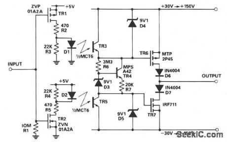
This circuit takes as an input a signal from a 5-V CMOS logic circuit and outputs a high voltage of the same polarity. The high-voltage supply can be varied from (30 V to ) 150 V without the need to change circuit components. The input voltage is applied to the gates of transistors TR1 and TR2.TR3 is optically coupled to D1 as is TR5 to D2. R5 limits the current through D2, while R3 and R4 reduce the affects of leakage current. The light transmitted by D1 turns TR3 on and discharges the gate-source capacitance of TR6, which turns TR6 off. At the same time, TR5 is off and a constant current produced by R6, R7, D3, and TR4 charges the gate-sourced capacitance of TR7, thus turning TR7 on.With TR7 on and TR6 off, the output is pulled close to the lower supply rail. When the input is high, TR1 is off and TR2 is on. Therefore, D2 conducts, which turns on TR5. With TR3 off and TR5 on, TR6 turns on and TR7 off. The output is pulled towards the higher supply rail. (View)
View full Circuit Diagram | Comments | Reading(681)
PULSE_TRAIN
Published:2009/7/9 4:19:00 Author:May
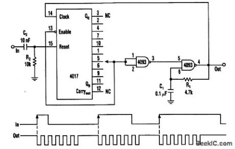
This circuit has a rate multiplier usmg a 4093 Schmitt trigger as an oscillator,driving a 4017 decadecounter. When a pulse present at the input(to C2)4017 is reset,output zero goes high,and outputs 1 to 9 go low.The oscillator(4093)starts runrung and the 4017 counts the pulses until the 4017 output(1 to 9)connected to pin 1 and 2 of the 4093 goes high.The osciffator IS inhibited and the output remains high until the next input pulse. (View)
View full Circuit Diagram | Comments | Reading(2803)
UNIPOLAR_TO_DUAL_SUPPLY_CONVERTER
Published:2009/7/9 4:17:00 Author:May
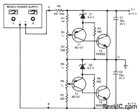
The outputs in this circuit are independently variable and can be loaded unsymmetrically. The output voltage remains constant, irrespective of load and changes. By varying potentiometers R2 or R6, the output voltages can be conveniently set. Outputs can be varied between 8 and 17 V, so that the standard ±9, ±12, and ±15 V settings can be made. This converter is designed for a maximum load current of 1 A and the output impedance of both supplies of 0.35 Ω. This circuit is not protected against shortcircuits, but Uses the protection provided by the dc input source. This circuit is ideal for biassing operation amplifier circuits. (View)
View full Circuit Diagram | Comments | Reading(570)
VOLTAGE_GAUGE
Published:2009/7/9 4:12:00 Author:May
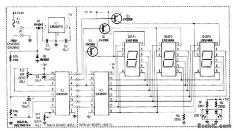
This circuit uses an RCA CA3162E (IC2) A/D converter. This converter has 12-bit output (BCD) which is sent to display decoder driver IC1. +5 V is obtained from IC1. R17 adjusts to 0 and R11 should be set to produce correct calibration of gauge unit. Displays are common cathode types. No limiting resistors are necessary because the output drivers are constant current. R15 and R16 sample the applied voltage (usually 8 to 18 V). LED1 is used to illuminate the gauge legend (Volts, Temp, etc.). (View)
View full Circuit Diagram | Comments | Reading(4088)
HIGH_VOLTAGE_BUCKING_REGULATOR
Published:2009/7/9 4:12:00 Author:May
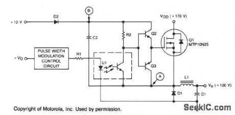
This circuit is basically the classic bucking regulator, except it uses a TMOS N-channel power FET for the chopper and creates its own supply for the gate control.The unique aspect of this circuit is how it generates a separate supply for the gate circuit, which must be greater than VDD. When power is applied, C2 charges, through D2, to + 12 V. At this time, Q1 is off and the voltage at point A is just below zero. When the pulse-modulated signal is applied, the optoisolator transistors, Q2 and Q3, supply a signal to Q1 that turns it on. The voltage at point A then goes to VDD, C2 back-biases D2, and the voltage at point B becomes 12 V above VDD.After Q1 is turned on, current starts to flow through L1 into C1, increasing until Q1 turns off. The current still wants to flow through L1, so the voltage at point A moves toward negative infinity, but is clamped by D1 to just below zero. Current flows less and less into C1, until Q1 turns on again. Q2 and Q3 drive Q1's gate between the voltages at point A and B, which is always a 12 V swing, so %g max. is never exceeded. For proper operation, the 12-V supply has to be established before the pulse-width modulator signal is applied. (View)
View full Circuit Diagram | Comments | Reading(716)
HIGH_INPUT_Z
Published:2009/7/9 4:11:00 Author:May
Suitablefor use as active probefor CRO,as electrometer,and for instrumentation applications Combination of unipolar and bipolar transistors gives desirable amplifying features of each solid-state device.-I. M. Gottlieb,A New Look at Solid-State Amplifiers,Ham Radio,Feb 1976,p 16一19.
(View)
View full Circuit Diagram | Comments | Reading(898)
DIGITAL_PRESSURE_GAUGE
Published:2009/7/9 4:10:00 Author:May
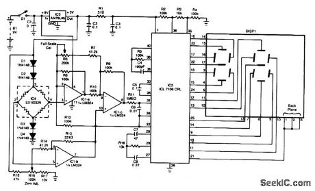
Using an intersil ICL 7106 A/D converter chip and an LED display module, this gauge uses a Sensym Corp. pressure transducer SX100pn (100 psi full scale) in a Wheatstone bridge configuration to drive an op amp (ICla, b, c) translator circuit that supplies a dc voltage to IC2 that is proportional to pressure. R6 sets the gain of ICIA (full-scale sensitivity) and R16 supplies a zero adjustment. IC3 provides regulated + 5 V to power the circuit. (View)
View full Circuit Diagram | Comments | Reading(3515)
ARC_JET_POWER_SUPPLY_AND_STARTING_CIRCUIT
Published:2009/7/9 4:07:00 Author:May
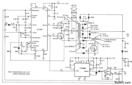
This circuit for starting arc jets and controlling them in steady operation is capable of high power efficiency and can be constructed in a lightweight form. The design comprises a pulse-width-modulated power converter, which is configured in a closed control loop for fast current control. The series averaging inductor maintains nearly constant current during rapid voltage changes, and thereby allows time for the fastresponse regulator to adjust its pulse width to accommodate load-voltage changes. The output averaging inductor doubles as the high-voltage pulse transformer for ignition. The starting circuit operates according to the same principle as that of an automobile ignition coil. When the current is interrupted by a transistor switch, the inductor magnetic field collapses, and a high-voltage pulse is produced. The pulse is initiated every 0.25 second until arc current is detected, then the pulser is automatically turned off. (View)
View full Circuit Diagram | Comments | Reading(1402)
| Pages:224/471 At 20221222223224225226227228229230231232233234235236237238239240Under 20 |
Circuit Categories
power supply circuit
Amplifier Circuit
Basic Circuit
LED and Light Circuit
Sensor Circuit
Signal Processing
Electrical Equipment Circuit
Control Circuit
Remote Control Circuit
A/D-D/A Converter Circuit
Audio Circuit
Measuring and Test Circuit
Communication Circuit
Computer-Related Circuit
555 Circuit
Automotive Circuit
Repairing Circuit