
Index 225
SUPPLY_VOLTAGE_SPLITTER
Published:2009/7/9 4:02:00 Author:May
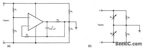
This simple circuit can convert a single supply voltage, such as a battery, into a bipolar supply. Sense resistors R1 and R2 establish relative magnitudes for the resulting positive and negative voltages. Their rail-to-rail value, of course, equals VSUPPLY. R4 and R5 represent the load impedances. For example, equalvalue sense resistors produce 1/2 VSUPPLY across each of the load resistors, R4 and R5. The op amp maintains these equal voltages by sinking or sourcing current through R3; the op amp's action is equivalent to that of variable conductances G1 and G2 in shunt with each load resistor. Choose a value for R3 so that the largest voltage across it, the greatest load-current mismatch, won't exceed the op amp's output-voltage capability for the application. You can add a buffer amplifier at the op amp's output to provide greater load currents. If you need bypass capacitors across the load resistors as well, connect a capacitor (dashed lines) to ensure that the amplifier remains stable. (View)
View full Circuit Diagram | Comments | Reading(805)
AC_VOLTAGE_REGULATOR
Published:2009/7/9 4:01:00 Author:May
View full Circuit Diagram | Comments | Reading(799)
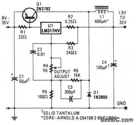
SLOW_TURN_ON_15_V_REGULATOR
Published:2009/7/9 4:00:00 Author:May
View full Circuit Diagram | Comments | Reading(964)
HIGH_CURRENT_INDUCTOULESSSWITCHING_REGULATOR
Published:2009/7/9 3:59:00 Author:May


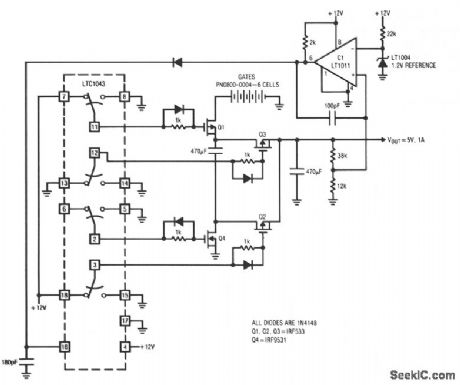
The LTC10432 switched-capacitor building block provides nonoverlapping complementary drive to the Q1 to Q4 power MOSFETs. The MOSFETs are arranged so that C1 and C2 are altemately placed in series and then parallel. During the series phase, the + 12 V battery's current flows through both capacitors, charging them, and fumishing load current. During the parallel phase, both capacitors deliver current to the load. Q1 and Q2 receive similar drive from pins 3 and 11. The diode-resistor networks provide additional nonoverlapping drive characteristics, preventing simultaneous drive to the series-parallel phase switches. Normally, the output would be one-half of the supply voltage, but C1 and its associated compo-nents close a feedback loop, forcing the output to 5 V. With the circuit in the series phase, the output heads rapidly positive. When the output exceeds 5 V, C1 trips, forcing the LTC1043 oscillator pin, trace D, high; this truncates the LTC1043's triangular-wave oscillator cycle. The circuit is forced into the parallel phase and the output coasts down slowly, until the next LTC1043 clock cycle begins. C1's output diode prevents the triangle down-slope from being affected and the 100-pF capacitor provides sharp transitions. The loop regulates the output to 5 V by feedback controlling the turn-off point of the series phase. (View)
View full Circuit Diagram | Comments | Reading(689)
POSITIVE_REGULATOR_WITH_NPN_AND_PNP_BOOST
Published:2009/7/9 3:56:00 Author:May
In the circuit, Q1 and Q2 are connected in the classic SCR or thyristor configuration. Where higher input voltages or minimum component count are required, the circuit for thyristor boost can be used. The thyristor is running in a linear mode with its cathode as the control terminal and its gate as the output terminal. This is known as the remote base configuration. (View)
View full Circuit Diagram | Comments | Reading(734)
EFFICIENT_NEGATIVE_VOLTAGE_REGULATOR
Published:2009/7/9 3:54:00 Author:May
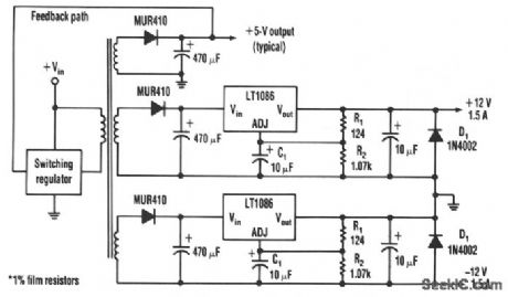
One way to provide good negative-voltage regulation is with a low-dropout positive-voltage regulator operating from a well-isolated secondary winding of switch-mode circuit transformer. The technique works with any positive-voltage regulator, although highest efficiency occurs with low-dropout types.Under all loading conditions, the minimum voltage difference between the regulator VIN and V0UT pins must be at least 1.5V, the LT1086's low-dropout voltage. If this requirement isn't met, the output falls out of regulation. Two programming resistors, R1 and R2, set the output voltage to 12 V, and the LT1086's servo the voltage between the output and its adjusting (ADJ) terminals to 1.25 V. Capacitor C1 improves ripple rejection, and protection diode D1 eliminates common-load problems.Since a secondary winding is galvanically isolated, a regulator's 12 V output can be referenced to ground. Therefore, in the case of a negative-voltage output, the positive-voltage terminal of the regulator connects to ground, and the -12 V output comes off the anode of D1. The VIN terminal floats at 1.5 V or more above ground. (View)
View full Circuit Diagram | Comments | Reading(2364)
NONLINEAR_PORENTIOMER_OUTPUTS
Published:2009/7/9 3:53:00 Author:May
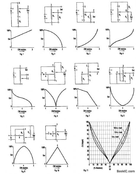
Using these illustrated conftgurations, various rotation output characteristics can be obtained from potentiometers and one or two resistors. (View)
View full Circuit Diagram | Comments | Reading(582)
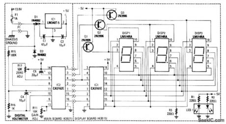
DIGITAL_FUEL_GAUGE
Published:2009/7/9 3:51:00 Author:May
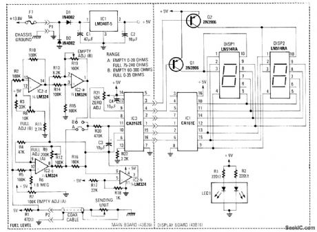
This circuit uses a digital voltmeter (formed from IC1 and IC3) to display fuel quantity as a percentage of a full tank. In order to work with two kinds of fuel sensors, low resistance = full. Where higher resistance full, IC2 forms a dc amplifier that has both inverting (path A) or noninverting (path B) outputs, and calibration adjustments for each path. (View)
View full Circuit Diagram | Comments | Reading(3554)
DIGITAL_VACUUM_GAUGE
Published:2009/7/9 3:47:00 Author:May
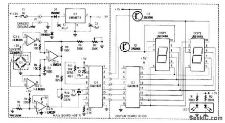
A bridge circuit is used to produce a signal from the output of vacuum sensor IC1. IC2b provides about a 0.2 V offset for IC4, the A/D converter. IC2b and d are voltage followers that drive differential amp IC2a. The output of this circuit is used to drive IC4 and IC1, the display drivers. (View)
View full Circuit Diagram | Comments | Reading(1712)
ELECTRONIC_VOICE_SUBSTITUTE
Published:2009/7/9 3:45:00 Author:May
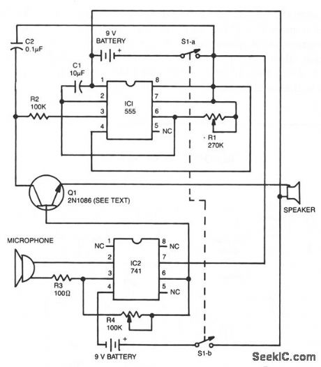
The 555 acts as the tone generator configured in the astable mode. Its pin 3, square-wave output is transformed into a triangle wave by R1 and C2. The voice's pitch is controlled by R1. Transistor Q1 can be 2N1086, 2N1091, or any other equivalent npn germanium type. Sounds are amplified by the 741, and the IC's output drives the transistor to saturation. When the transistor is in the saturated state, the triangle wave is able to reach the speaker, and your new voice can be heard. (View)
View full Circuit Diagram | Comments | Reading(1007)
WATER_TEMPERATURE_GAUGE
Published:2009/7/9 3:41:00 Author:May
This gauge is similar to the miscellaneous temperature gauge, except that a thermostat is used as a sensing element. (View)
View full Circuit Diagram | Comments | Reading(1246)
DIGITAL_OIL_PRESSURE_GAUGE
Published:2009/7/9 3:39:00 Author:May
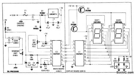
This gauge uses a sensor in conjunction with R1 to develop a dc voltage proportional to oil pressure. IC1 and IC2 form a two-digit DVM. Q1 and Q2 are display selectors for the multiplexed display. IC1 provides the necessary +5V to the circuitry. Calibration is via R11 and zero adjust via R17. (View)
View full Circuit Diagram | Comments | Reading(1290)
LOW_COST_3_A_SWITCHING_REGULATOR
Published:2009/7/9 3:30:00 Author:May
View full Circuit Diagram | Comments | Reading(1060)
FREQUENCY_VOLTAGE_CONVERTER
Published:2009/7/9 3:29:00 Author:May
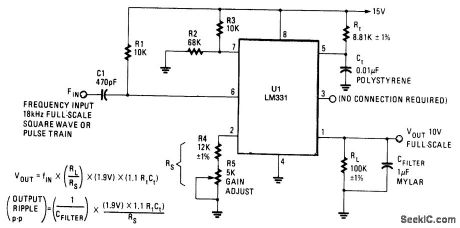
A dc output that is proportional to frequency can be derived with this circuit. It is useful for analog frequency meter or tachometer applications. (View)
View full Circuit Diagram | Comments | Reading(2188)
FREQUENCY_VOLTAGE_CONVERTER_WITH_SAMPLE_AND_HOLD
Published:2009/7/9 3:25:00 Author:May
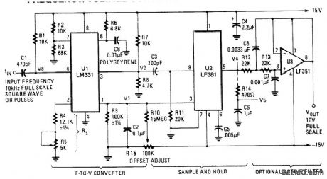
U1 is a frequency/voltage converter, feeding sample-and-hold circuit using an LF381. An LF351 pro-vides 10-V full-scale output. The circuit produces 1-V/kHz output. (View)
View full Circuit Diagram | Comments | Reading(788)
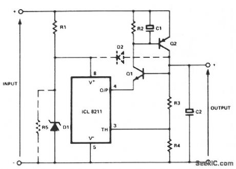
POSITIVE_REGULATOR_WITH_PNP_BOOST
Published:2009/7/9 3:23:00 Author:May


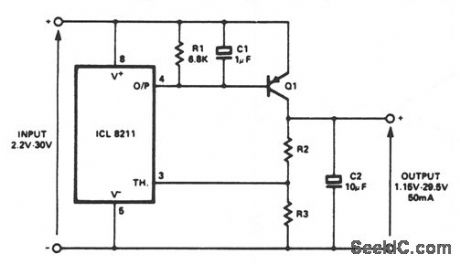
The IC8211 provides the voltage reference and regulator amplifier, while Q1 is the series pass transistor. R1 defines the output current of the IC8211, while C1 and C2 provide loop stability and also act to suppress feedthrough of input transients to the output supply. R2 and R3 determine the output voltage as follows:output supply. R2 and R3 determine the output voltage as follows:In addition, the values of R2 and R3 are chosen to provide a small amount of standing current in Q1, which gives additional stability margin to the circuit.Where accurate setting of the output voltage is required, either R2 or R3 can be made adjustable. If R2 is made adjustable, the output voltage will vary linearly with the shaft angle; however, if the potentiometer wiper was to open the circuit, the output voltage would rise. In general, therefore, it is better to make R3 adjustable, since this gives fail-safe operation. (View)
View full Circuit Diagram | Comments | Reading(1513)
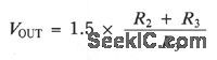
FREQUENCY_VOLTAGE_CONVERTER_WITH_OPTOCOUPLER_INPUT
Published:2009/7/9 3:21:00 Author:May
In this circuit, the input from IC2 optocoupler is fed to the comparator input of the AD650 (Analog Devices or Maxim Electronics) V/F converter. This internally generates a pulse that is fed to the op amp, which outputs a dc voltage that is proportional to frequency. Component values are shown in the figure. (View)
View full Circuit Diagram | Comments | Reading(982)
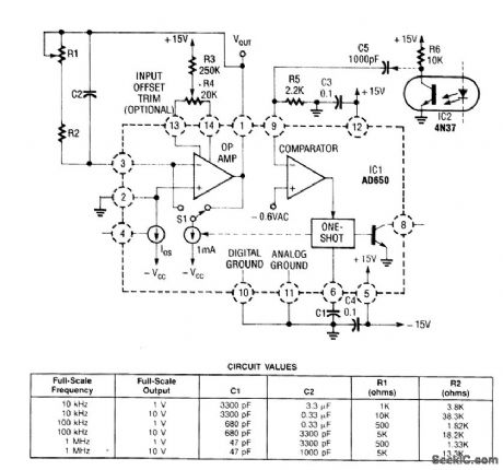
DIALED_PHONE_NUMBER_VOCALIZER
Published:2009/7/9 3:21:00 Author:May
By vocalizing the numbers and symbols of its keypad, the phone provides an audible confirmation that is useful to the blind. The serial-interface, 2 K-byte x 8-bit ROM (IC4) stores programmed sequences of instructions that are executed by the speech-processor chip IC2-manufactured by the General Instrument Corp. When you depress a key, tone-dialing chip IC1 issues the corresponding number of pulses at its DP output. Counter IC5 totals the pulses, and IC6 latches the resulting 4-bit digital word. This word, converted to serial format by IC2, becomes an address that selects a block of memory within IC4. (View)
View full Circuit Diagram | Comments | Reading(1033)
AC_LINE_VOLTAGE_ANNOUNCER
Published:2009/7/9 3:16:00 Author:May
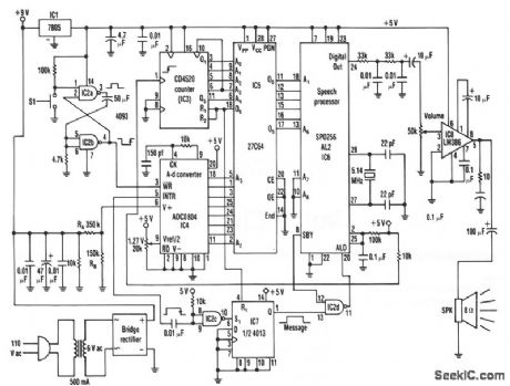
The range of this ac-voltage monitor is 100 to 140 Vac, with a resolution of 1 V. The speech processor interprets an 8-bit binary input code from an analog-to-digital converter. The processor's pulse-code-modulated output then passes through a filter and an amplifier before driving the circuit's speaker to vocalize the corresponding number. Each time switch S1 is pressed, the speech-processor program enunciates the monitored voltage readings from 100 to 140 V, depending on the code at the input of a 27C64 EPROM.The voltage-monitoring circuit consists of a bridge rectifier, filter capacitors, and a 10-KΩ load resistor. A divider, RA and RB, limits the input voltage to a maximum 2.55 V. The a/d converter, IC4, then sends the voltage reading to the 27C64 EPROM, ICS. Pressing S1 sends a negative transient pulse to the write, WR, input of the a/d converter, IC4, which initiates a 100-μs conversion process. (View)
View full Circuit Diagram | Comments | Reading(1880)
HIGH_STABILITY_10_V_REGULATOR
Published:2009/7/9 3:12:00 Author:May

View full Circuit Diagram | Comments | Reading(624)
| Pages:225/471 At 20221222223224225226227228229230231232233234235236237238239240Under 20 |
Circuit Categories
power supply circuit
Amplifier Circuit
Basic Circuit
LED and Light Circuit
Sensor Circuit
Signal Processing
Electrical Equipment Circuit
Control Circuit
Remote Control Circuit
A/D-D/A Converter Circuit
Audio Circuit
Measuring and Test Circuit
Communication Circuit
Computer-Related Circuit
555 Circuit
Automotive Circuit
Repairing Circuit