
Index 234
3_digit_ISUP2_SUPL_DPM_with_LCD_interface
Published:2009/7/20 21:53:00 Author:Jessie
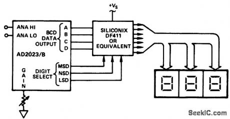
3-digit I2L DPM with LCD interface (courtesy Analog Devices, Inc.). (View)
View full Circuit Diagram | Comments | Reading(575)
12_digit_TTL_multiplexed_planar_gas_discharge_display
Published:2009/7/20 22:10:00 Author:Jessie
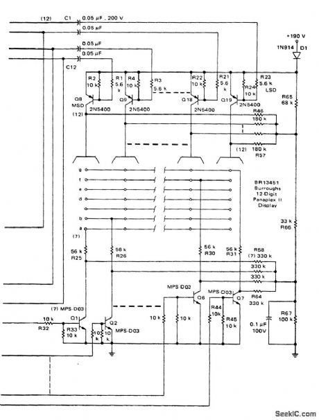
12-digit TTL multiplexed planar gas discharge display (courtesy Motorola Semiconductor Products Inc.). (View)
View full Circuit Diagram | Comments | Reading(599)
INVERTING_SAMPLE_AND_HOLD
Published:2009/7/20 22:09:00 Author:Jessie
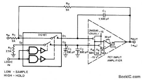
Total offset error can be adjusted to much less than 1 mV in 2N5545 FET-input opamp by using compensation circuit R3-C2-C3 with DG181 JFET analog switch. Switch operation occurs consistently at constant voltage, reducing aperture time jitter. Designed for high-speed sample-and-hold requirements.- Analog Switches and Their Applications, Siliconix, Santa Clara,CA,1976,p7-59. (View)
View full Circuit Diagram | Comments | Reading(702)
DERIVATIVE_SLOPE_SAMPLING
Published:2009/7/20 22:07:00 Author:Jessie
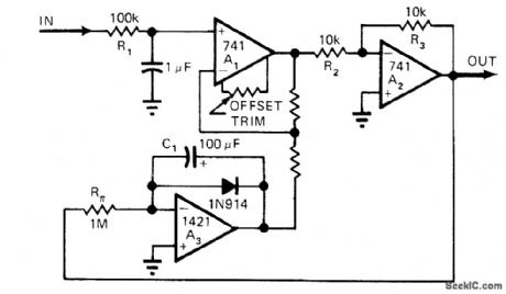
Analog derivative circuit forces voltage across C1 to follow slowly changing input signal. Current required to keep capacitor voltage equal to signal volt-age is proportional to rate of change of signal voltage. RCA 3033 FET-input opamp will work equally as well as Teledyne Philbrick 1421 shown. Careful selection of values for Rπ and C1 will set rate limit that will reject spikes.-R. E. Bober, This Derivative Circuit Handles Slowly Varying Signals, EDN Magazine, Jan. 20, 1976, p82. (View)
View full Circuit Diagram | Comments | Reading(730)
JFET_SAMPLE_AND_HOLD
Published:2009/7/20 21:51:00 Author:Jessie
Logic voltage is applied simultaneously to sample-and-hold JFETs. By matching input impedance and feed-back resistance and capacitance, errors due to ON resistance of JFETs are minimized.- FET Databook, National Semiconductor, Santa Clara, CA, 1977, p 6-26-6-36. (View)
View full Circuit Diagram | Comments | Reading(0)
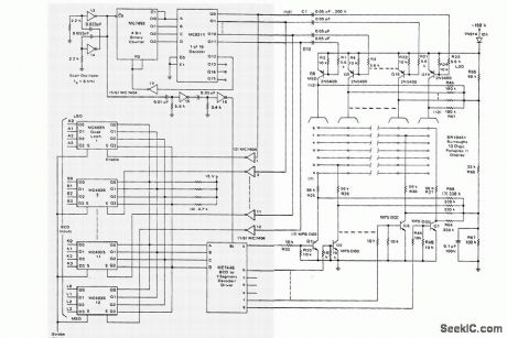
6_digit_fluorescent_triode_display
Published:2009/7/20 22:31:00 Author:Jessie
6-digit fluorescent triode display (courtesy Motorola Semiconductor Products Inc.). (View)
View full Circuit Diagram | Comments | Reading(494)
CMOS_to_4_digit_incandescent_display_interface
Published:2009/7/20 22:27:00 Author:Jessie
CMOS to 4-digit incandescent display interface(Courtesy Motorola Semiconductor Products Inc.). (View)
View full Circuit Diagram | Comments | Reading(622)
SERIES_DIODE_MAGNETRON_MODULATOR
Published:2009/7/21 0:08:00 Author:Jessie
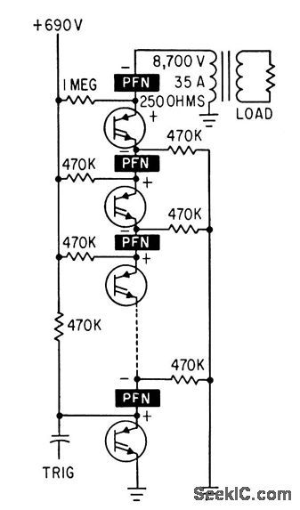
In variation of spark-gap modulator, 25 pnpn diodes in series with pulse-forming networks (PFN) are switched by trigger and resulting voltage transient to supply 8,700 v at 35 amp to load. Success depends on availability of 700-v diodes.-F. A. Gateka and M. L. Embree, Semiconductor Modulators for Modern Magnetrons, Electronics, 35:37, p 42-45. (View)
View full Circuit Diagram | Comments | Reading(715)
PULSE_TIME_MODULATOR_USES_TWO_QUAD_RANT_MULTIPLIER
Published:2009/7/21 0:07:00 Author:Jessie
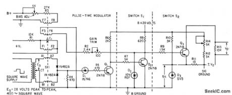
Output transistor Q3 servas as series switch driven by Q2 and magnetic modulator to give accurate analog multiplication.-W. R. Seegmiller, Accurate Analog Computation with Pulse-Time Modulation, Electronic, 35:13, p 54-57. (View)
View full Circuit Diagram | Comments | Reading(669)
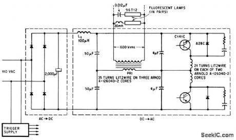
CHOPPER_MODULATOR
Published:2009/7/21 0:06:00 Author:Jessie
Reduces output signal null level by balancing out zero input signal. Null levels con be maintained in microvolt region by proper shielding. Long time drift stability is less than 1 my referred to output. Used with strain gage and other low-level transducer signals.-L. S. Klivans, Modulators for Automatic Control Systems, Electronics, 31:1, p 82-84. (View)
View full Circuit Diagram | Comments | Reading(843)
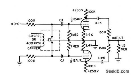
BALANCED_TRIODE_SINE_WAVE_MODULATOR
Published:2009/7/21 0:04:00 Author:Jessie
Gives sinusoidal output without filtering-Can be used for either open-loop or error signal modulation when high input impedance and low-distortion sinusoidal output are required. Long-term drift stability is less than 1 mv per hour referred to output.-L. S. Klivans, Modulators for Automatic Control Systems, Electronics, 31:1, p 82-84. (View)
View full Circuit Diagram | Comments | Reading(632)
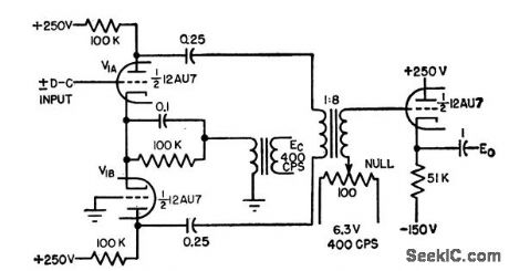
LINEAR_PWM_FOR_05_TO_175_V
Published:2009/7/21 0:03:00 Author:Jessie
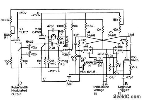
Tubes V4 and V5 form bistable mvbr that will accept modulation voltage range of 350:1 from 0.5v to175 v, at point A. V3 is Miller ntegrator.Wilh 0.055 mfd for C1, pulse lengths are 61 and 173 millisec for limits of modulation voltage. Linearity is nearly perfect.-J,E,Frecker, A Pulse Width modulator, EEE, 10:12,p 28-300 (View)
View full Circuit Diagram | Comments | Reading(501)
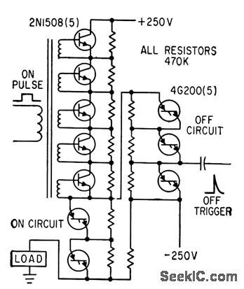
2_KV_MODULE_OF_MAGNETRON_MODULATOR
Published:2009/7/21 0:02:00 Author:Jessie
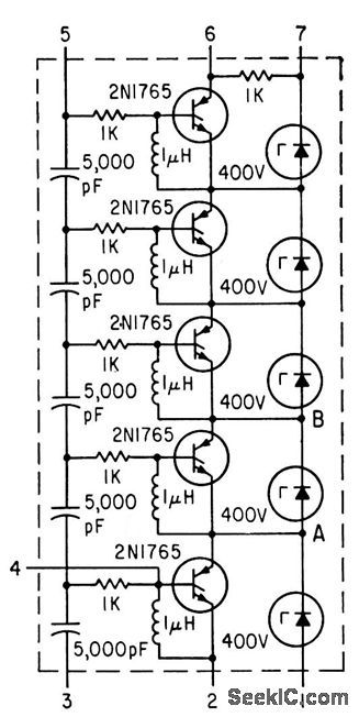
With terminal 6 at +2,000 v, voltage-regulator diodes maintain 400 v across each pnpn transistor. Lowest transistor receives 0.5.amp, 3-v trigger at its gate.-F. A. Gateka and M. L. Embree, Semiconductor Modulators for Modern Magnetrons, Electronics, 35:37, p 42-45. (View)
View full Circuit Diagram | Comments | Reading(822)
HYBRID_DIODE_TUBE_PULSE_MODULATOR
Published:2009/7/21 0:01:00 Author:Jessie
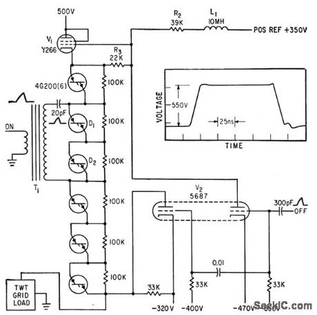
Closely spaced pulses of any length, with 15-nsec rise and fall times al 550 V and 1.4 amp are produced for modulating traveling-wave tube by combining fast response of four-layer diodes with current-handling capabilities of tubes.-E. H. Heckman, Three New Approaches to Pulse Modulation, Electronics, 36:18, p 62-64. (View)
View full Circuit Diagram | Comments | Reading(605)
TRANSFORMER_COUPLED_SERIES_D_C_MODU_LATlON
Published:2009/7/21 Author:Jessie
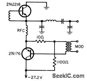
Eliminates need for bulky modulation transformer and reduces envelope distortion when used in 27-Mc CB transmitter. Modulation power required is 0.35 mw. Chief disadvantage is that voltage source must be twice that of conventional collector-modulated transmitter.-B. Rheinfelder, Modulation Techniques for Transistorized A.M Transmitters, EEE, 11:7, p 54-57. (View)
View full Circuit Diagram | Comments | Reading(572)
F_M_P_M
Published:2009/7/20 23:59:00 Author:Jessie
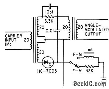
Angle modulator gives phase modulation below 500 cps and frequency modulation above. Voltage-variable capacitor HC-7005 gives phase angle change of up to 25° at 1Mc.-A. C. Todd, P. Schuck, and H. M. Sachs, Using Voltage-Variable Capacitors in Modulator Design, Electronics, 34;3, p 56-59. (View)
View full Circuit Diagram | Comments | Reading(798)
TRANSISTOR_DIODE_PULSE_MODULATOR
Published:2009/7/20 23:58:00 Author:Jessie
Four-layer diodes used in series give rise times faster than turn-on limes of transistors, for pulse modulation of traveling-wave tubes and other devices al repetition rates up to 100 kc, with 5-microsec pulses and 3-mkrosec pulse spacings.-E. H. Heckman, Three New Approaches to Pulse Modulation, Electronics, 36:18, p 62-64. (View)
View full Circuit Diagram | Comments | Reading(706)
DIODE_SWITCHED_IF_FILTER
Published:2009/7/8 5:06:00 Author:May
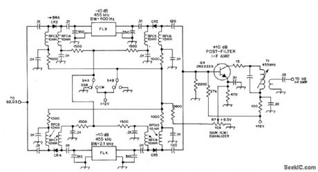
Used in 1.8-2 MHz communication receiver having wide dynamic range 1N914 diodes select collins mechanical filter F455FD-04 FL3 (400-Hz bandwidth) or F455FD-25 FL4(2.5-kHz bandw)Reverse biasis applied to nonconducting diodes to lesson leakage through switching diodes Filteris located between IF preamρ and main IF strip of receiver Two-part article gives all other circuits of receiver,-D.DeMaw,His Eminence-the Receiver,QST,Part 1-June 1976,p 27-30(Part2-July 1976,p 14-17). (View)
View full Circuit Diagram | Comments | Reading(857)
ZERO_SUPPRESSION
Published:2009/7/8 5:06:00 Author:May
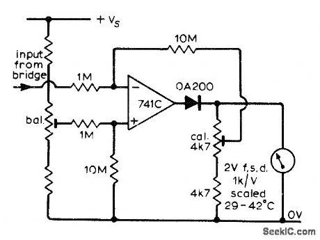
Opamp is used in in, verting configuration at output of temperature-sensing bridge, so noninverting input of opamp can be used for suppressing meter zero when temperature range for application is 29 to 42°C .Calibration control is set for gain of about 17.2 to make meter direct-reading. Article gives operation details and methods of improving temperature stability of circuit.-R. J. Isaacs, Optimizing Op-Amps, Wireless World, April1973, p 185-186. (View)
View full Circuit Diagram | Comments | Reading(0)
_CONSTANT_SPEED_MOTOR_DRIVER
Published:2009/7/8 5:05:00 Author:May
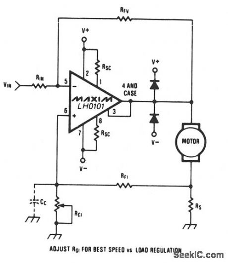
When the torque load on the motor increases, its current increases. This current increase is sensed across RS, and positive feedback is applied to the noninverting terminal of the LH0101, thereby increasing the motor voltage to compen-sate for the increased torque load. With the proper amount of positive feedback, the motor-speed variation can be kept below 1% from no load to full load. (View)
View full Circuit Diagram | Comments | Reading(768)
| Pages:234/471 At 20221222223224225226227228229230231232233234235236237238239240Under 20 |
Circuit Categories
power supply circuit
Amplifier Circuit
Basic Circuit
LED and Light Circuit
Sensor Circuit
Signal Processing
Electrical Equipment Circuit
Control Circuit
Remote Control Circuit
A/D-D/A Converter Circuit
Audio Circuit
Measuring and Test Circuit
Communication Circuit
Computer-Related Circuit
555 Circuit
Automotive Circuit
Repairing Circuit