
Index 232
DOLBY_B_NOISE_REDUCTION_CIRCUIT_IN_ENCODE_MODE
Published:2009/7/8 22:04:00 Author:May
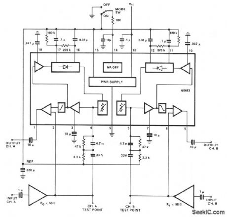
View full Circuit Diagram | Comments | Reading(728)
DOLBY_B_C_NOISE_REDUCTION_SYSTEM
Published:2009/7/8 22:03:00 Author:May
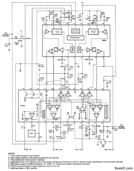
View full Circuit Diagram | Comments | Reading(641)
ANALOG_MULTIPLEXER_WITH_BUFFERED_INPUT_AND_OUTPUT
Published:2009/7/8 22:01:00 Author:May
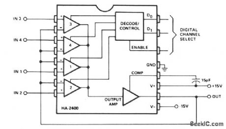
This circuit is used for analog signal selection or time division multiplexing. As shown, the feedback signal places the selected amplifier channel in a voltage follower (noninverting unity gain) configuration, and provides very high input impedance and low output impedance. The single package replaces four input buffer amplifiers, four analog switches with decoding, and one output buffer amplifier. For low-level input signals, gain can be added to one or more channels by connecting the (-) inputs to a voltage divider between output and ground. The bandwidth is approximately 8 MHz, and the output will slew from one level to another at about 15.0 V per μs.
Expansion to multiplex 5 to 12 channels can be accomplished by connecting the compensation pins of two or three devices together, and using the output of only one of the devices. The enable input on the unselected devices must be low.
Expansion to 16 or more channels is accomplished easily by connecting outputs of four 4-channel multiplexers to the inputs of another 4-channel multiplexer. Differential signals can be handed by two identical multiplexers addressed in parallel. Inverting amplifier configurations can also be used, but the feedback resistors might cause crosstalk from the output to unselected inputs.
(View)
View full Circuit Diagram | Comments | Reading(1907)
VHF_TONE_TRANSMITTER
Published:2009/7/8 22:00:00 Author:May
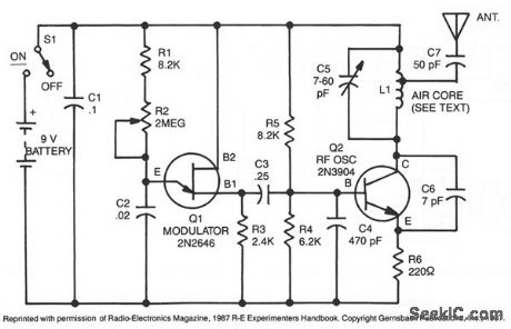
The range of this transmitter is about 50 feet with a short whip antenna. The tone generator, is made up of a unijunction transistor, Q1, and R1, R2, R3, and C2. Transistor Q1 pulses on and off at a rate determined by the time constant of R1 and R2, together with the capacitance of C2 and the BI-emitter junction of Q1. Trimmer potentiometer R2 determines the frequency of the tone generated and allows a range of approximately 100 Hz to over 5 kHz.Transistor Q2 is the rf oscillator. Its frequency is set by tuned circuits consisting of L1, C5, C6, and the interelectrode capacitance of Q2. The values shown will give a tuning range of about 55 to 108 MHz. Capacitor C6 provides positive feedback from the emitter to the collector of Q2, for oscillation. The audio tone generated by Q1 is applied to the base of Q2, causing the collector current to vary at the frequency of the tone, yielding an amplitude-modulated (AM) signal. This, in turn, varies Q2's collector-to-emitter capacitance, which makes up part of the tuned circuit, and causes the output frequency to vary similarly, producing a frequency-modulated (FM) signal, as well. The rf signal is coupled to the antenna through capacitor C7.Coil L1 consists of five turns of #18 bare wire, close-wound on a piece of 1/4-inch wooden dowel. The length of the winding is about 1/4 inch. One end of capacitor C7 is soldered to the coil, one turn away from the 9-V supply end, and the other capacitor end is connected to the antenna. To adjust the vertical height and linearity of a TV set, place the tone transmitter near the set and use R2 to select the number of horizontal bars to be displayed. Once the picture is steady and the bars are sharp, adjust the set's vertical controls, so that all the bars are of the same height and are evenly spaced.The fact that both AM and FM signals are generated makes it possible to use this circuit to check almost any receiver within the transmitter's frequency range. A TV set's sound section (discriminator) will reject the AM portion of the signal, but its video section will respond to it. Similarly, the TV sound section and FM receivers will respond to the FM signal produced. (View)
View full Circuit Diagram | Comments | Reading(719)
THREE_CHANNEL_MULTIPLEXER_WITH_SAMPLE_AND_HOLD
Published:2009/7/8 22:00:00 Author:May
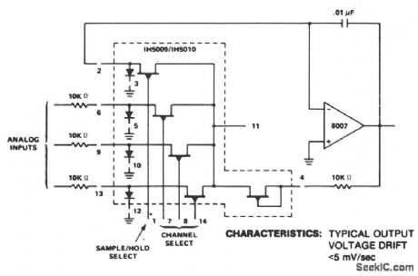
View full Circuit Diagram | Comments | Reading(617)
DEMULTIPLEXER
Published:2009/7/8 21:56:00 Author:May
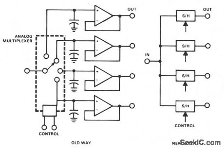
This circuit reconstructs and separates analog signals which have been time-division multiplexed. The conventional method, shown on the left, has several restrictions, particularly when a short dwell time and a long, accurate hold time is required. The capacitors must charge from a low-impedance source through the resistance and current-limiting characteristics of the multiplexer. When holding, the high-impedance lines are relatively long and subject to noise pickup and leakage. When FET input buffer amplifiers are used for low leakage applications, severe temperature offset errors are often introduced. (View)
View full Circuit Diagram | Comments | Reading(2578)
LOW_COSR_FOUR_CHANNEL_MULTIPLEXER
Published:2009/7/8 21:55:00 Author:May
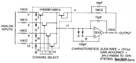
View full Circuit Diagram | Comments | Reading(566)
FM_SNOOPER
Published:2009/7/8 21:55:00 Author:May
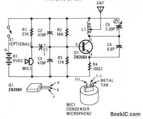
The FM Snooper is an FM transmitter that radiates a continuous wave whose frequency is alteredaccording to the sound waves striking the microphone. An ordinary FM broadcast recelver detects thetransmitter’s output carner. When 9-V battery,B1,is connected,a brief Surge of current flows from the collector to the emitter of Q1,causing an alternating current,shock oscillation in the resonant LC circuit,to flow back and forth between L1 and C5. So,by varying the value of C5,you can tune the oscillations to the exact frequency desired。Although tuning capacitor C5 accounts for the major part of the tuning capacitance,the capacitance between the base and the collector of Q1 has a small,but noticeable,effect on the oscillati frequency. That capacitance,which is known as the junction capacitance,is not a fixed value,but instead vanes when the voltage on the base of the transistor vanes. Sound waves striking the microphone induce a voltage that vanes in time with the sound. That voltage is applied via C1 to the base ofQ1,thereby frequency modulating the transmitter. (View)
View full Circuit Diagram | Comments | Reading(3204)
50_OHM_LINE_DRIVER
Published:2009/7/8 21:54:00 Author:May
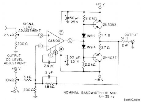
CA3100 bipolar MOS opamp operates as high-slew-rate wideband amplifier that provides 18 V P-P into open circuit or 9 V P-P into 50-ohm transmission line. Slew rate is 28 V/μs.- Circuit Ideas for RCA Linear 1Cs, RCA Solid State Division, Somerville, NJ, 1977, p 13. (View)
View full Circuit Diagram | Comments | Reading(2218)
1_OF_15_CASCADED_VIDEONUX
Published:2009/7/8 21:54:00 Author:May

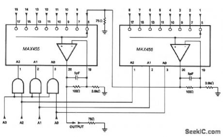
Two MAX455s can be cascaded to form a 1 of 15 video MUX by connecting the output of one MUX to one of the input channels of a second MUX. Although the two devices are usually close to one another, the output of the first MUX should be terminated to preserve its bandwidth. (View)
View full Circuit Diagram | Comments | Reading(522)
TWO_LEVEL_MULTIPLEXER
Published:2009/7/8 21:52:00 Author:May
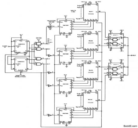
When a large number of channels are multiplexed, the outputs of two or more multiplexers can be connected together and each multiplexer sequentially enabled. In the inhibit mode, the multiplexer draws less power and its output and inputs act as open circuits. Theoretically, an infinite number of channels can be accommodated in this way; in practice, the accumulated output capacitance and leakage of many paralleled multiplexers limits the speed and accuracy of the system. A much better method is the two-level multiplex system. The two-level system has a bank of high-speed switches at the output which sequentially switch between the four DG406s. Each DG406 is able to switch during the time the other three are being interrogated. The DG406s contribute leakage and capacitance at the output only, when they are switched on by the DG411-1/4 of the time. The two-level multiplex system is very useful in communications links, high-speed interfacing with comparators, or wherever a large number of channels must be multiplexed at high speeds.
(View)
View full Circuit Diagram | Comments | Reading(1518)
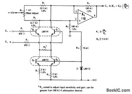
±34_V_COMMON_MODE_RANGE
Published:2009/7/8 21:39:00 Author:May
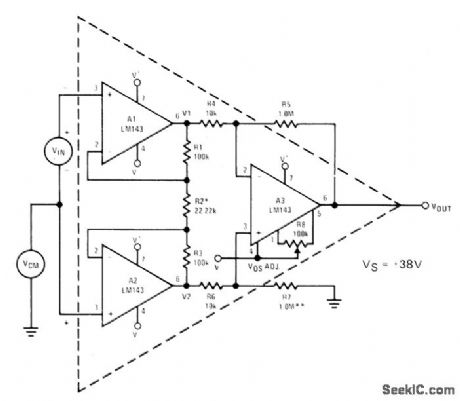
Interconnections shown for three LM143 high-voltage opamps give equivalent of single differentialinput opamp having wide common-mode range, high input impedance, and gain of 1000.Adjust R2 to trim gain. Adjust R7 for best common-mode rejection. With 10 K load, frequency response is down 3 dB at 8.9 kHz.- Linear Applications, Vol, 2, National Semiconductor, 'OUT Santa Clara, CA, 1976, AN-127, p 2-3. (View)
View full Circuit Diagram | Comments | Reading(752)
0_35_MHz_WITH_GAIN_OF_10
Published:2009/7/8 21:14:00 Author:May

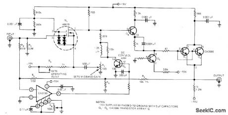
Wkleband amplifier handles inputs up to 100 mV P-P and drives 1-kilohm load, to meet requirements of oscilloscope preamps, instrumentation and pulsesignal amplifiers, and video signal processots. High-frequency gain is provided by 40673 dual-gate MOSFET. Low-frequency gain with DC stabilization is provided by CA3130 CMOS opamp. Transistors Q1-Q5 are part of CA3086 transistor-array IC. Values of R3 and R4 in feedback path establish amplifier gain. R6 sets operating point of N1 for 10-mA drain current. Base resistor ofQ3 is 1 kilohm.-H. A. Wittlinger, CMOS Op Amp, MOSFET Implement Wideband Amplifier, EDN Magazine, June 20, 1977, p 114. (View)
View full Circuit Diagram | Comments | Reading(1598)
HIGH_GAIN_WITH_WIDE_BANDWIDTH
Published:2009/7/8 20:50:00 Author:May
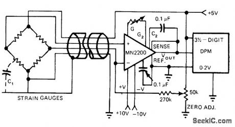
Micro Networks MN2200 instrumentation amplifier is used with strain gage to create digital-readout torque wrench.Strain gages having nominal impedance of 120 ohms are bonded to torque-sensing member at 450 to longitudinal axis, so gages in opposite bridge arms are under simultaneous tension or compression for given direction of torque.Bridge power is taken from 5-V digital panel meter supply. Instrumentation amplifier will work with any voltage from ±5 to ±15 V. Variable gain-adjust resistor G (l0-turn 50K pot) is set so DPM reads 200 ft-lb of torque at full scale in increments of 0.1 ft-lb.-R. Dulls, Instrumentation Amplifiers-They're Great Problem Solvers When Correctly Applied, EDN Magazine, Sept. 5, 1977, p 133-135. (View)
View full Circuit Diagram | Comments | Reading(617)
DIGITAL_THERMOMETER_
Published:2009/7/8 5:49:00 Author:May
Diode D2 serves assensor for driving A/D converter directly,eliminating temperature-drift er o rs normally asso-ciated with amplifiers. Can be calibrated over temperature range of -199°to 199° in either Fahrenheit or Celsius scales. Aceuracy is about 1°-H Wurzburg and M Hadley,Digital Thor-mometer Circumvents Drift,Electronics.Jan 5,1978,p 176-177
(View)
View full Circuit Diagram | Comments | Reading(1660)
0_15_MHz_WITH_100_dB_CMR_
Published:2009/7/8 5:35:00 Author:May
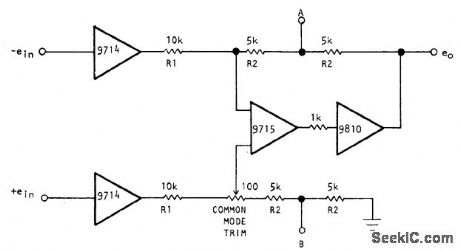
Differential inputs are applied to Optical Electronics 9715 opamp through 9714 voltage followers. Currentbooster using 9810 opamp raises load current to ±100 mA. Complete amplifier has very high differential and common-mode input impedance. Common-mode rejection can be trimmed to greater than 100 dB at 1 kHz for unity gain.Gain is determined by value of resistor RG connected between points A and B and is equal to(2R2/R1)(1 + 2R2/RG). Settling time is 500 ns.Accuracy is maintained from -550C to +85 0C-''Instrumentation Ampliffer, Optical Electronics, Tucson, AZ, Application Tip 10240. (View)
View full Circuit Diagram | Comments | Reading(819)
WIND_SPEED
Published:2009/7/8 5:21:00 Author:May

Developed to give magnitude of wind velocity over wide range of values when its two measured vectors are' expressed as voltages. Output is in Iogarithmig form for easy adaptation to data processorg. N-S and E-W veetor voltages from straitgage sensors ate converted to normalized values \/X and VYwhich are squared by MC1495L four-quadrant transconductance multipliers. Output currents are then summgct, and HA2705 opamp is used as differential current-to-voltage converterto obtain Vss as sum-of-squares ofVX and VY. Range covered is 1-100 mph. Article covers operation of circuit in detail.-J. A. Connolly and M.B.Lundberg.Analog Multipliers Determine True Wind Speed, EDN Magazine, April 20, 1974, p 69-72. (View)
View full Circuit Diagram | Comments | Reading(1194)
TEMPERATURE_TRANSDUCER_INTERFACE
Published:2009/7/8 5:17:00 Author:May
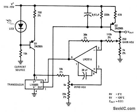
Output of National LX5600 temperature-sensing transducer is inverted, level-shifted, and given extra voltage gain of 4 to give required output of0 to +5 V for telemetry system or instrumentation recorder. Q1 furnishes constant current to thermometer, and Q2 provides inverting function. Resulting output signal is reinverted by LM201A opamp connected through zero-adjust divider to pin 3 which provides voltage reference.-P. Lefferts, A New Interfacing Concept; the Monolithic Temperature Transducer, National Semiconductor, Santa Clara, CA, 1975, AN-132, p 3. (View)
View full Circuit Diagram | Comments | Reading(768)
STEPPING_MOTOR_DRIVE
Published:2009/7/8 5:16:00 Author:May
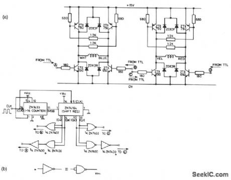
The circuit shown in Fig. 62-15A is designed to drive a 15-V, two-phase, bipolar stepping motor, providing a bidirectional single level voltage across each winding at currents of up to 9.6 A. The circuit consists of two identical transistor bridge stages employing complementary npn and pnp devices.The transistor conduction sequence is determined by external control logic, and the circuit will interface directly with standard TTL, suitable controllogic system is illustrated in Fig.62-15B.
(View)
View full Circuit Diagram | Comments | Reading(938)
IC_FOR_DIFFERENTIAL_THERMOCOUPLE
Published:2009/7/8 5:16:00 Author:May

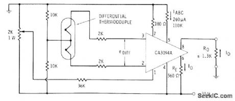
Amount of heat sensed by differential thermo-couple is proportional to voltage between pins 2 and a of CA3094A programmable power switch/amplifier. Input swing of ±26 mV gives single-ended output current range of ±8.35 mA.-E. M. Noll, Linear IC Principles, Experiments, and Projects, Howard VV. Sams, lndi-anapolis, IN, 1974, p 314.
(View)
View full Circuit Diagram | Comments | Reading(716)
| Pages:232/471 At 20221222223224225226227228229230231232233234235236237238239240Under 20 |
Circuit Categories
power supply circuit
Amplifier Circuit
Basic Circuit
LED and Light Circuit
Sensor Circuit
Signal Processing
Electrical Equipment Circuit
Control Circuit
Remote Control Circuit
A/D-D/A Converter Circuit
Audio Circuit
Measuring and Test Circuit
Communication Circuit
Computer-Related Circuit
555 Circuit
Automotive Circuit
Repairing Circuit