
Electrical Equipment Circuit
Index 14
Philips SW2000 powered subwoofer circuit diagram 1
Published:2011/9/2 1:01:00 Author:Ecco | Keyword: Philips , powered subwoofer
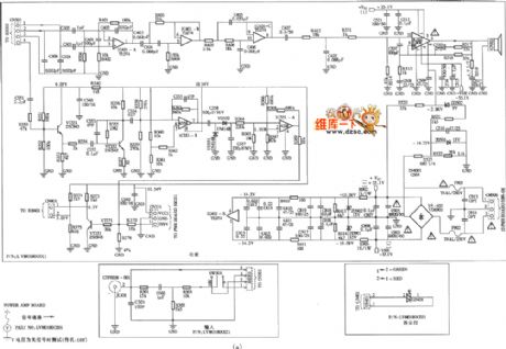
View full Circuit Diagram | Comments | Reading(6557)
CD4017 ultrasonic pest repeller circuit diagram
Published:2011/9/9 1:51:00 Author:Ecco | Keyword: ultrasonic pest repeller
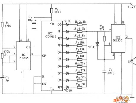
View full Circuit Diagram | Comments | Reading(7834)
Charger principle circuit diagram
Published:2011/8/31 22:14:00 Author:Ecco | Keyword: Charger principle
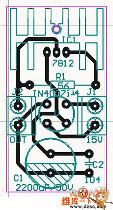
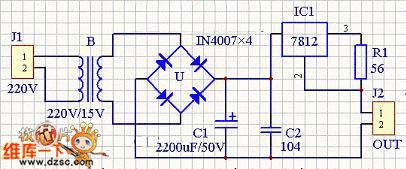
It uses 1 / 10 rated capacity ( 145 mA charging current) to charge for 14 to 16 hours. The charger charging current is about 170 mA, and the charging time is about 12 hours. The required components are: a transformer with power being about 10W and the secondary winding voltage between 12 ~ 15V; 7812 three-terminal voltage regulator integrated circuit; 4 IN4008 diodes ( or a 1A/200V bridge rectifier ), a 2200UF/50V electrolytic capacitor and a 0.1UF homopolar capacitor; a 56 ohm resistor; a battery box which can put four batteries; a piece of board, and many wires.
(View)
View full Circuit Diagram | Comments | Reading(2256)
Samsung CE959 microwave circuit diagram
Published:2011/9/14 2:44:00 Author:Ecco | Keyword: Samsung, microwave
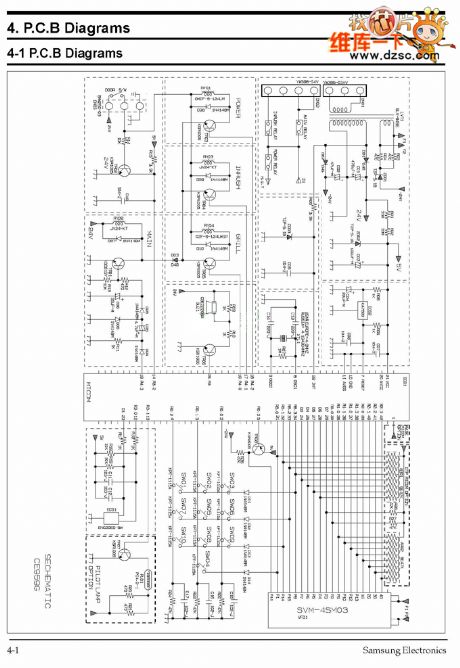
View full Circuit Diagram | Comments | Reading(2595)
Samsung CE959 microwave circuit diagram 2
Published:2011/9/14 2:50:00 Author:Ecco | Keyword: Samsung , microwave
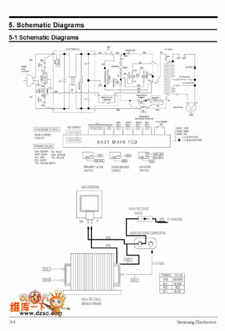
View full Circuit Diagram | Comments | Reading(3686)
Video Preamplified Circuit Diagram
Published:2011/9/14 0:26:00 Author:Zoey | Keyword: Video Preamplified
SID2141X is a kind of video preamplifier IC and it is widely used in a variety of domestic and imported color monitors.
The SD2141X integrated circuit contains a three-color signal processing circuit, a three-color gain control circuit, and a blanking signal processing circuit,tec. The circuit uses 20-pin dual in-line package, and the circuits have been used in LGCB56lBN color monitors, its foot arch function and data of the integrated circuit have been listed in Table 1. (View)
View full Circuit Diagram | Comments | Reading(1193)
SHB6605 Power-Drive Integrated Circuit Diagram
Published:2011/9/13 0:12:00 Author:Zoey | Keyword: SHB6605 Power Drive, Integrated Circuit Diagram
As a power driver IC, SHB6605 is widely used in air conditioners controlled by microcomputers, such as Changhong, Chinese style series air conditioners.1 FeaturesSHB6605 IC consists a power driver circuit, a speed adjustment circuit, and other auxiliary functions circuits. It is typically used to drive the indoor fan motor, for operation of different speeds .2 Pin functions and DataSHB6605 IC pin 13 single in-line package for Changhong KFR-36GW / D air-conditioner , the pin functions of integrated circuit and data have been listed in Table 1
(View)
View full Circuit Diagram | Comments | Reading(1127)
Circuitry Design for Electronic Lock, Sauna Lock, Cabinet Lock and Hotel Lock
Published:2011/9/12 23:50:00 Author:Zoey | Keyword: Electronic Lock, Sauna Lock, Cabinet Lock, Hotel Lock
Our company has always been concentrating on researching and developing a series of intelligentized, digitized and networked innovative products. Based on MCU Embedded technology, we have introduced methods of dealing with and controlling digital circuits, we have most systematic and strongest technology and application of digital circuits. By right of precious and scientific research and development, systematic test and experiment, we have mastered radiofrequency-series technology and attained corresponding independent intellectual rights. Regarding Electronic Technology as the kernel of our company, we observe the guideline of combining scientific research with industry, combing chip design with its application, we stand firmly on principle of Equality and Mutual Benefit, and redouble our efforts to offer our customers the best service. (View)
View full Circuit Diagram | Comments | Reading(1018)
Anti-toll-fraud sound and light annunciator circuit diagram
Published:2011/9/13 6:48:00 Author:Vicky | Keyword: anti-toll-fraud, sound and light annunciator circuit
Anti-toll-fraud sound and light annunciator circuit diagram is shown in the above picture. The picture is an anti-toll-fraud sound and light warning circuit. It is assembled in the junction box of service entrance conductor. It normally does not consume power or affect the normal work of telephone. When anyone uses the line to make calls stealthily, the luminous diode shrinks, and the annunciator sound sends out warning. Because the voltage of the exterior line of the telephone is higher, the diode VD1~VD4 adopts 1N4004 type diode. Triode V1 and V2 use small-power high reverse voltage tube, such as types (PNP type, note that the polarity of the power supply should be changed) of 2N5551 (it’s reverse voltage is 160V) or 2N5401. The relay K adopts 4098 of small size, and the work voltage uses 3V. (View)
View full Circuit Diagram | Comments | Reading(2466)
Anti-toll-fraud circuit diagram
Published:2011/9/7 5:02:00 Author:Vicky | Keyword: Anti-toll-fraud circuit
Anti-toll-fraud circuit is shown in the above picture. The circuit in the picture is a anti-toll-fraud circuit which also performs collinear security feature. It is mainly made up of illegal parallel examine circuit, noise interference circuit, linear privacy-keeping circuit. The circuit is assembled between the telephone device and the exterior line. When there is toll-fraud, the circuit starts working and sends strong noise to the line, which makes the pulse or double audio frequency sent by the toll-fraud unable to be received. Meanwhile, the anti-toll-fraud indication light is lighted, and the host can track the caller. (View)
View full Circuit Diagram | Comments | Reading(1072)
Circuit diagram of electronic code lock with self-locking function
Published:2011/9/7 1:23:00 Author:Vicky | Keyword: electronic code lock , self-locking function
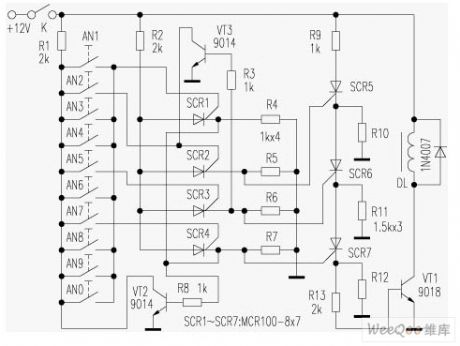
The circuit is shown as in the above picture. Silicon controlled rectifiers SCR5, SCR6, and SCR7 are the main control components of the code lock. If the three-digit number code keys are pressed down in the right sequence (AN2, AN5 and AN7 in this case) , the silicon controlled ractifiers SCR2, SCR3, and SCR4 are conducted in turn, thus to conduct SCR5, SCR6, and SCR7 in turn. VT1 is saturated and conducnted. Electromagnet starts move. Meanwhile, SCR4 is conducted when the AN7 is pressed down, and then VT2 is saturated and conducted, which makes those keys not work then.
(View)
View full Circuit Diagram | Comments | Reading(1747)
Wireless telephone adaptor circuit diagram
Published:2011/9/9 7:42:00 Author:Vicky | Keyword: wireless, telephone adaptor
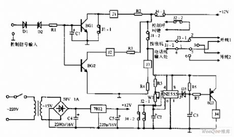
Wireless telephone adaptor circuit is shown in the above picture. The composition of the wireless telephone adaptor is very simple and the cost is very low, while the function is complete and practical. Its functions are listed below: after adding the adaptor, the average wireless can dial two external lines of different region arbitrarily in accordance with one’s demands, which equals two wireless telephone actually. As the user with many extensions, it can also realize making calls among the extensions, and the function of tallback. (View)
View full Circuit Diagram | Comments | Reading(2054)
Application Circuit of LCD TV Power
Published:2011/9/3 10:19:00 Author:Zoey | Keyword: Application Circuit, LCD TV Power
PLC810PG group and LLC lineless controller integrate with high pressure half-bridge driver. Picture 1 shows the circuit of PLC810PC power supply configuration.
PFC of PLC810PG uses a general continuous current mode that does not have to refer to sine signal, in this way, costs of the system and exterior accessories are reduced.
DC-DC controller drives the LLC resonance topologies.
Dead band time of LLC switch in PLC810PG can be adjusted by an exterior resistance.
PFC converter’s frequency is limited in LLC to reduce the interference of noise and electromagnetism.
This design also refers to elementary exception handles of PFC and LLC. Dynamic adjustment can be achieved by consulting phase proportion of LLC to PFC.
(View)
View full Circuit Diagram | Comments | Reading(1226)
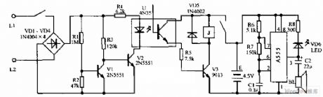
Pulse Charge Time Relay Circuit
Published:2011/9/3 10:03:00 Author:Zoey | Keyword: Pulse Charge, Time Relay
Pulse Charge Time Relay Circuit (View)
View full Circuit Diagram | Comments | Reading(1004)
SID2141X Video Preamplified Circuit Diagram
Published:2011/9/3 21:28:00 Author:Zoey | Keyword: Video Preamplified
SID2141X is a kind of video preamplifier ICand it iswidely used in a variety of domestic and imported color monitors. The SD2141X integrated circuit contains a three-color signal processing circuit, a three-color gain control circuit, and ablanking signal processing circuit,tec. Thecircuit uses20-pin dual in-line package, and the circuits have been used in LGCB56lBN color monitors,its foot arch function and dataof the integrated circuit have been listed in Table 1. (View)
View full Circuit Diagram | Comments | Reading(1008)
Simplified Long-Distance Call Lock Circuit Diagram
Published:2011/9/7 0:43:00 Author:Vicky | Keyword: Simplified Long-Distance Call Lock Circuit
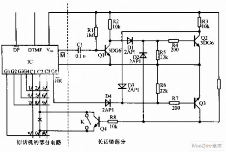
Simplified long-distance call lock is shown in the above picture. The lock can lock out the long-distance call without affecting the original function. It ispower-consuming, but it has very good compatibility. If switch K is placed as the picture shows, first dial the number “0”,, and you’ll find the “0” can not be dialed and the long-distance call can not be made while it does not affect dialing “0” when making local calls; if K is placed to the left, then the lock does not function. (View)
View full Circuit Diagram | Comments | Reading(1685)
Simplified Anti Toll Fraud Circuit Diagram
Published:2011/9/7 0:43:00 Author:Vicky | Keyword: Simplified Anti Toll Fraud Circuit
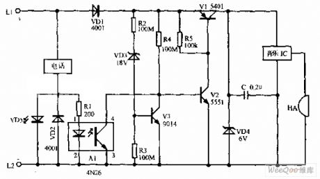
Simplified anti toll fraud circuit is shown in the above picture. The picture is a simplified anti toll fraud circuit. When the telephone is made normally, the indication light is luminous. When anyone wiretaps and makes calls, the circuit will give out fierce alarming sound which prevents the telephone from regular usage. The input lines of the circuit can be divided into positive and negative. The output lines can be connected with the telephone arbitrarily. (View)
View full Circuit Diagram | Comments | Reading(1242)
Bipolar Telephone Circuit Diagram
Published:2011/9/7 0:46:00 Author:Vicky | Keyword: Bipolar Telephone Circuit
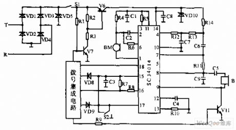
Bipolar Telephone circuit is shown in the above picture. The circuit is a typical applied circuit of bipolar telephone IC SC34014. The circuit is simple, and the lowest work voltage is 1.5V when the call isunder usage. 34014 has a stabilized output voltage of 1.2V (providing working voltage for electret microphone); it has a stabilized DC voltage of 3.3V and current output of 550μ, and the current increases to 2mA when dialing. (View)
View full Circuit Diagram | Comments | Reading(2322)
Seashore biofeedback therapy device circuit diagram
Published:2011/9/8 21:00:00 Author:Lucas | Keyword: Seashore biofeedback, therapy device
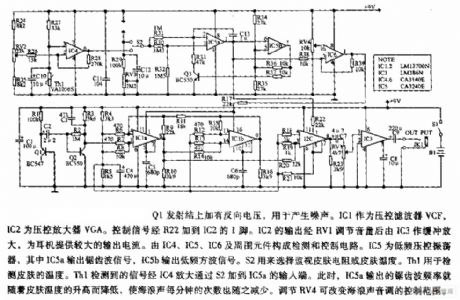
The Q1 emitter junction is added reverse voltage for generating noise. IC1 is used as a voltage-controlled filter VCF, and IC2 is the voltage-controlled amplifier VGA. Controlling signal is added to the pin 1 of IC2 by R22. IC1's output is adjusted by RV1, then buffered and amplified by IC3 to provide a larger output current for the headphones. The IC4, IC5, IC6 and the surrounding components form the detection and control circuit. IC5 is the low-frequency voltage-controlled oscillator, and IC5a outputs sawtooth signal, IC5b outputs low-frequency square wave signal. S2 is used to select monitoring skin resistance or skin temperature.
(View)
View full Circuit Diagram | Comments | Reading(2646)
ECG FM demodulator circuit diagram
Published:2011/9/8 20:51:00 Author:Lucas | Keyword: ECG FM demodulator
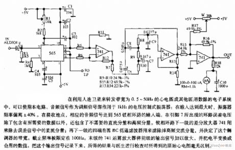
The circuit is suitable for satellite to transmit the ECG with bandwidth in 0.5 ~ 50Hz or other medical data in electronic systems. Audio signal is used as FM signal source applied to the 1KHz voltage controlled oscillator: when the input is maximum, the oscillator frequency deviation is ± 40%. In the receiving place, the corresponding audio signal is sent to the input of 565 PLL. The loop error voltage on pin 7 contains the necessary, in addition, it also contains the DC components and high-frequency components which are not necessary.
(View)
View full Circuit Diagram | Comments | Reading(3303)
| Pages:14/126 1234567891011121314151617181920Under 20 |
Circuit Categories
power supply circuit
Amplifier Circuit
Basic Circuit
LED and Light Circuit
Sensor Circuit
Signal Processing
Electrical Equipment Circuit
Control Circuit
Remote Control Circuit
A/D-D/A Converter Circuit
Audio Circuit
Measuring and Test Circuit
Communication Circuit
Computer-Related Circuit
555 Circuit
Automotive Circuit
Repairing Circuit