
Electrical Equipment Circuit
Index 19
Basic Voltage Regulator Composed Of Zener Diode
Published:2011/8/14 8:21:00 Author:Robert | Keyword: Basic, Voltage, Regulator, Zener Diode
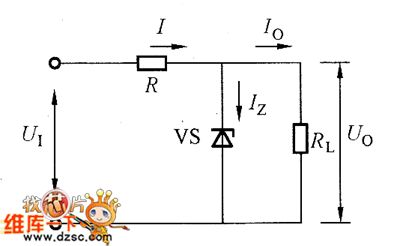
The picture shows the basic voltage regulator composed of zener diode. In the circuit, the R is current-limiting resistor. The RL is loading resistor. The VS is zener diode which is used as the adjustable element. It should note the connecting method when using, which is that it should be reversely connected to the circuit. The circuit regulator process is simply introduced here: when the U1 is increasing to cause the Uo to be bigger, the VS's current Iz is increasing, so the voltage drop on the R is increasing. Thus it keeps the stability of Uo. The same, when the U1 reduces to cause the Uo to reduce, the Iz is also reduced. Then the voltage drop on R is reduced to keep the stability of Uo.
The picture shows the basic voltage regulator composed of zener diode. (View)
View full Circuit Diagram | Comments | Reading(2456)
Capacitance Input Type Rectifier Circuit
Published:2011/8/14 1:54:00 Author:Robert | Keyword: Capacitance, Input, , Rectifier
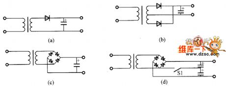
The capacitance input type rectifier circuit has the single-phase half-wave rectifier circuit, single-phase middle-tap full-wave rectifier circuit, single-phase bridge rectifier circuit and voltage doubler rectifier circuit and so on. The picture (a) shows the single-phase half-wave rectifier circuit. The circuit is simple, but its output current is small and ripple is big. The picture (b) shows the single-phase middle-tap full-wave rectifier circuit. It is suitable for medium and small power supply circuits. The picture (c) shows the bridge rectifier circuit. It has more two diodes than the middle-tap rectifier circuit. But its transformer power is just 0.7 times of the middle-tap rectifier circuit. (View)
View full Circuit Diagram | Comments | Reading(2457)
LT1773 Application Circuit
Published:2011/8/11 6:41:00 Author:Robert | Keyword: Application
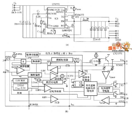
The LT1773 application circuit is shown in the picture. (View)
View full Circuit Diagram | Comments | Reading(1122)
TL1681/LTC1698 Application Circuit
Published:2011/8/11 6:39:00 Author:Robert | Keyword: Application
The TL1681/LTC1698 application circuit is shown in the picture. (View)
View full Circuit Diagram | Comments | Reading(933)
Flyback Type Converter Circuit Composed Of MAX5021
Published:2011/8/14 3:39:00 Author:Robert | Keyword: Flyback, Converter
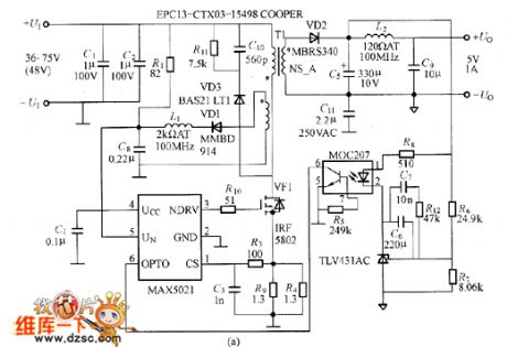
The picture shows the flyback type convertor composed of MAX5021. The MAX5021 is a isolated power PWM current-type integrated controller with wide input voltage range. It is suitable for the remote communication. This controller works under the 262kHz fixed oscillation frequency switching and it could reduce the noise efficiently. It has a big hysteresis feature and low starting current. It also has the low-voltage closing and locking function and so on. If MAX5021 is used in the power supply with wide voltage input range and low output power, it could reduce the power supply's power consumption.
The picture shows the flyback type converter circuit composed of MAX5021. (View)
View full Circuit Diagram | Comments | Reading(2001)
Low Noise Convertor Circuit Composed Of LT1777
Published:2011/8/13 22:19:00 Author:Robert | Keyword: Low, Noise, Convertor
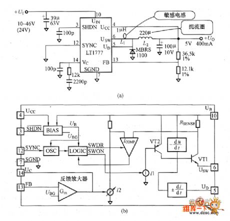
The picture shows the convertor circuit composed of LT1777. This is a low noise non-isolated buck type DC-DC convertor with output of 5V/400mA. The LT1777 has internal di/dr and dta/dr limiting circuit, switching circuit with rated current peak value of 700mA, current control mode short-circuit protection circuit. Its oscillation frequency is 100kHz. The picture (c) shows the efficiency features at input voltage of 12V, 24V, 36V. These are the tested efficiency under the inductor L1 of 0uH, 1uH, 2.2uH. If connecting the sensing inductor it could reduce the noise. But from the efficiency feature curve we know that the internal power consumption would increase and the efficiency would be lower. So it should note this problem when selecting the sensing inductor. (View)
View full Circuit Diagram | Comments | Reading(957)
Boost Voltage Convertor Circuit Composed Of LTC1700
Published:2011/8/14 3:41:00 Author:Robert | Keyword: Boost, Voltage, Convertor
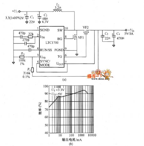
The picture shows the convertor circuit composed of LTC1700. This is a simple circuit to convert the 3.3V voltage to 5V voltage. The LTC1700 is a PWM integrated controller with MSOP package, 530kHz working frequency and current mode. Its effciency could be maximum 95%. And it also has the new function that not using resistor to detect main MOSFET current. So it needn't the sensing resistor. In the circuit shown in picture (a), it only consume 180pA current in the dormancy mode. So it is best suitable for the portable type devices standby power-saving mode. For the practical products, if the input/output ports connect the LC filter, it would make the noise lower.
(View)
View full Circuit Diagram | Comments | Reading(955)
Convertor Circuit Composed Of TPS54610
Published:2011/8/13 6:19:00 Author:Robert | Keyword: Convertor
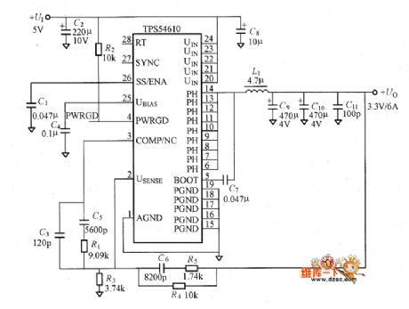
The picture shows the low input voltage to low output voltage DC-DC convertor. It uses the PWM comtrol method and the oscillation frequency is set to be 350kHz or 550kHz. Its input voltage is 5V and output is 3.3V/61A.
The TPS54610 uses TSSOP package. It has internal high-end MOSFET and low-end MOSFET. All the semiconductor devices needed by the power are modularized. It can make up the new buck convertor. So its conversion efficiency is very high.
The picture shows the convertor circuit composed of TPS54610. (View)
View full Circuit Diagram | Comments | Reading(1155)
Voltage Driving MOSFET Grid Electrode Principle Circuit
Published:2011/8/17 7:01:00 Author: | Keyword: Voltage, Driving, MOSFET, Grid, Electrode, Principle
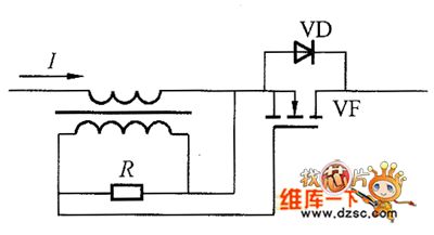
The MOSFET grid electrode driving principle circuit by using the current transformer secondary winding induced voltage is shown in the picture. The current would firstly circulate through the MOSFET parasitic diode. So the current transformer secondary winding would generate the induced voltage. When this voltage is beyond the threshold voltage, it would charge the MOSFET grid electrode. And the current would be conducted through MOSFET channel. Firstly the current which through the parasitic diode would generate the voltage drop about 1V. But when it is through the MOSFET channel, only its conducted resistance would generate a low voltage drop and there are no other voltage drop. That is the synchronous rectification. The principle circuit in the picture can not be used in the high-speed switching rectifier without any changing. (View)
View full Circuit Diagram | Comments | Reading(1262)
Synchronous Rectifier Buck Chopper Circuit
Published:2011/8/13 6:10:00 Author:Robert | Keyword: Synchronous, Rectifier, Buck, Chopper
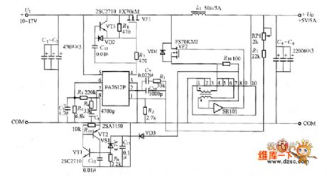
The circuit, which uses the synchronous rectifier buck chopper and has the output of 5V/5A, is shown in the picture. In the circuit, VF2 is the MOSFET used for synchronous rectifier. The SR101 is synchronous driving module. If connecting the diode VD1's positive electrode to the ground it would make up the traditional buck chopper circuit.
The picture shows the synchronous rectifier buck chopper circuit. (View)
View full Circuit Diagram | Comments | Reading(1802)
DC-DC Convertor Circuit Composed Of BIC1421
Published:2011/8/11 6:37:00 Author:Robert | Keyword: DC-DC, Convertor
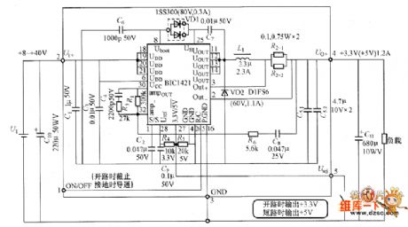
The DC-DC convertor circuit composed of BIC1421 is shown in the picture. (View)
View full Circuit Diagram | Comments | Reading(1100)
Practical Switch Voltage Regulator Power Supply Circuit With Positive Incentives Convertor Method
Published:2011/8/12 18:43:00 Author:Robert | Keyword: Practical, Switch, Regulator, Power Supply, Positive, Incentives, Convertor, Method
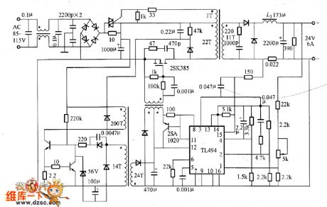
The practical switch voltage regulator power supply circuit is shown in the picture. The positive incentives convertor method's main features are:1.The transformer winding's primary and secondary has the same polarity.2.When VT1 is connected, the current i1 would be through Np. At the same time the output side has current i2 conducted, and the output current is Io. Also the inductor L is cumulating the energy.3.When the VT1 is disconnected, the L's opposite EMF would make the current conducted through VD2.4.The output side rectifier circuit is inductor input type whose switching frequency is beyond 100kHz.
The picture shows the practical switch voltage regulator power supply circuit with positive incentives convertor method. (View)
View full Circuit Diagram | Comments | Reading(1405)
The Li-ion battery drive white light LED circuit composed of LT3202 electric charge pump
Published:2011/8/18 7:43:00 Author: | Keyword: Li-ion battery, white light LED, electric charge pump
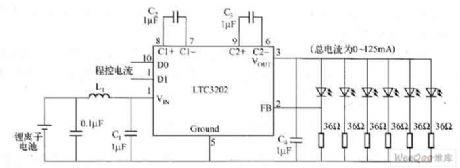
LTC3202 is an electric charge pump without gates which is produced by Linear Technology Corp., in the figure is the Li-ion battery drive white light LED circuit composed of LT3202 electric charge pump. To solve the problem of noise, LTC3202 is equipped with linear regulation technology, which can make sure the converting capacitance charge and discharge volume meet the need of the loading current, and it can keep it at the constant volume in each period, so they won't generate the audio weight.
Figure The Li-ion battery drive white light LED circuit composed of LT3202 electric charge pump (View)
View full Circuit Diagram | Comments | Reading(2557)
Absorbing Capacitor Charging And Discharging Control Circuit
Published:2011/8/14 1:31:00 Author:Robert | Keyword: Absorbing, Capacitor, Charging, Discharging, Control
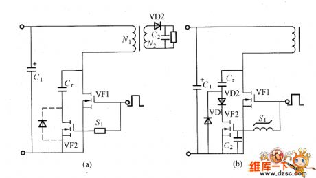
In the circuit shown in picture (a), VF1 is the primary side main MOSFET. The pulses from the PWM integrated controller can make it working in connected/disconnected mode. To make the VF2's connected/disconnected time be opposite to VF1, it adds the bidirectional time delay circuit S1. Now if the VF1 is in disconnected mode, the VF2 is in connected mode, the absorbing capacitor Cr would charge to the voltage between VF1's drain electrode and source electrode. So it also absorb the surge voltage on VF1. After the delay time, which is determined by the time delay circuit, the VF2 is disconnected. But at this time, the Cr two ports' voltage is equal to the voltage on VF1. So it is the zero-voltage and zero-current switching devices disconnected mode. (View)
View full Circuit Diagram | Comments | Reading(1504)
MAX639 Basic Application Circuit
Published:2011/8/11 6:34:00 Author:Robert | Keyword: Basic, Application
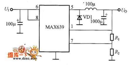
The picture shows the MAX639 basic application circuit. (View)
View full Circuit Diagram | Comments | Reading(1099)
MAX730 Series Integrated Voltage Regulator Internal Equivalent Circuit
Published:2011/8/11 6:30:00 Author:Robert | Keyword: Series, Integrated, Voltage, Regulator, Internal, Equivalent

The MAX730 series integrated voltage regulator internal equivalent circuit is shown in the picture. (View)
View full Circuit Diagram | Comments | Reading(1193)
MAX730 Basic Application Circuit
Published:2011/8/11 6:27:00 Author:Robert | Keyword: Basic, Application
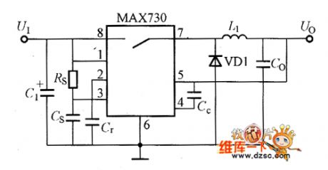
The MAX730 basic application circuit is shown in the picture. (View)
View full Circuit Diagram | Comments | Reading(876)
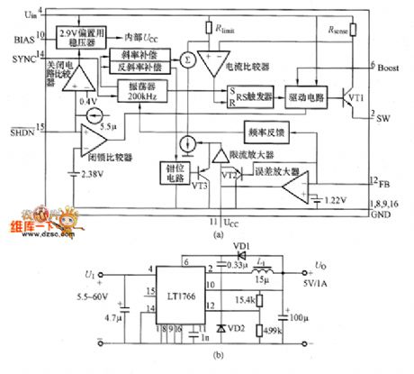
LT1766 Application Circuit
Published:2011/8/12 18:22:00 Author:Robert | Keyword: Application

The picture (a) shows the LT1766 internal equivalent circuit. In the chip it has the 200kHz oscillator, driving circuit, switch tube and other all function circuits which are needed by the buck voltage converter. The oscillation frequency is 20.0Hz and the internal-chip power transistor VT1's peak current is 1.5A. The picture (b) shows the buck voltage DC-DC converter composed of LT1766. It would convert the 5.5~60V input voltage to the 5V/1A output. This circuit's feature is wide input voltage range which is from 5.5 to 60V. It can be used in high-voltage car electronic devices, battery charger, distributed power supply and so on. (View)
View full Circuit Diagram | Comments | Reading(1006)
LT1109/LT1109A Internal Equivalent Circuit And Application Circuit
Published:2011/8/13 21:50:00 Author:Robert | Keyword: Internal, Equivalent, Application
The LT1109/LT1109A is low-power-consumption DC-DC convertor. Its output voltage has fixed three types which are 5V, 12V and adjustable output voltage. Its current consumption is maximum 550pA. For the 5V fixed type its output current is 100mA. For 12V fixed output current it is 60mA. It can control the logic voltage level to close the ports to make the power stop working. It uses 8-pin SOP, DIP and 3-pin T092 (only LT1109) and other packages.
The LT1109/LT1109A internal equivalent circuit diagram and aplication circuit is shown in the picture. The chip has internal 1.25V reference voltage generator and comparator. (View)
View full Circuit Diagram | Comments | Reading(1118)
Motor brake circuit diagram
Published:2011/8/11 1:35:00 Author:Ecco | Keyword: Motor brake
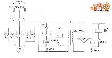
The motor brake circuit is composed of the power transformer T, rectifier diodes VD1 ~ VD4, variable resistor R, capacitor C, relay K, AC contactors KM1 and KM2 and start button S1, Stop button D2, and it is shown as the chart. Adjusting the resistor R can change the braking time of motor M to avoid excessive braking caused by motor reversal. R uses the sealed variable resistor. C selects the aluminum electrolytic capacitor with voltage in 50V. VD1 ~ VD4 select the 1N400l ~ 1N4007 type silicon rectifier diodes. K selects the small 12V relay.
(View)
View full Circuit Diagram | Comments | Reading(4477)
| Pages:19/126 1234567891011121314151617181920Under 20 |
Circuit Categories
power supply circuit
Amplifier Circuit
Basic Circuit
LED and Light Circuit
Sensor Circuit
Signal Processing
Electrical Equipment Circuit
Control Circuit
Remote Control Circuit
A/D-D/A Converter Circuit
Audio Circuit
Measuring and Test Circuit
Communication Circuit
Computer-Related Circuit
555 Circuit
Automotive Circuit
Repairing Circuit