
Electrical Equipment Circuit
Index 7
M1040 centerless grinding machine circuit
Published:2012/8/11 1:12:00 Author:Ecco | Keyword: centerless grinding machine
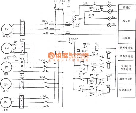
The centerless grinding machine is composed of grinding wheel, guide wheel , cooling, lubrication and hydraulic motor, and the circuit is shown in the figure. Before launching the grinding wheel motor 1M, the lubrication pump motor 3M should be started firstly to make the spindle dynamic bearing of grinding wheel fill with lubricating oil, then the oil returning make the floats rise, then the flowing relay KA's contacts are connected in order to start grinding wheel motor 1M. If the oil disappears, the device will be automatically stopped.
(View)
View full Circuit Diagram | Comments | Reading(3634)
Hair dryer circuit
Published:2012/8/1 2:35:00 Author:Ecco | Keyword: Hair dryer
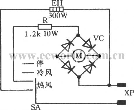
XP is thepower plug. EH is the 300W heating wire. R is the dropping resistor. VC is the bridge rectifier, and SA is thegear switch.
(View)
View full Circuit Diagram | Comments | Reading(8145)
Two-speed fan control circuit
Published:2012/8/1 2:06:00 Author:Ecco | Keyword: Two-speed fan , control circuit
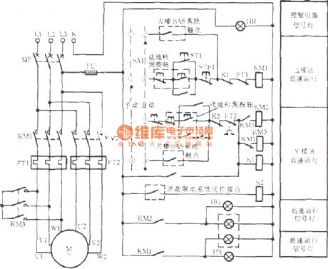
The two-speed exhausting fancomposed ofpole-changing adjustable speed motor is widely used in high-rise and underground buildings. Usually it runs at low speed; when the fireisbroke out, itcan be swicthed by manual, fire -place control systems or BAS system to high-speed operationautomatically to be used as exhausting fan. The circuit is shown as the chart.
(View)
View full Circuit Diagram | Comments | Reading(4643)
4096 bits CCDP drive circuit
Published:2011/4/15 5:39:00 Author:May | Keyword: 4096 bits, CCDP drive
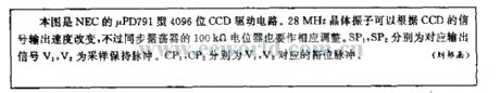
This diagram is NEC μPD791 type 4096 bits CCD drive circuit. 28MHz crystal oscillator can change according to CCD signal output speed. But 100kΩ potentiometer of lock-in oscillator should be adjusted accordingly. SP1, SP2 separately is corresponding signal. V1, V2 is sample hold pulse. CP1, CP2 separately is V1, V2 corresponding phase impulse. (View)
View full Circuit Diagram | Comments | Reading(1356)
Electronic stuttering appliance circuit
Published:2011/11/9 21:45:00 Author:May | Keyword: Electronic stuttering appliance
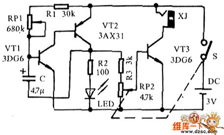
Electronic stuttering appliancecircuit is shown in the diagram, in fact, itis an electronic sound light metronome, and it utilizes rhythmed sound and light to stabilize emotion, and people will speak along with voice light rhythm to make them speak smooth gradually toreach the purpose to cure stammer.
In order to easier making, this text uses cheap components. The triodes'β value in the principle circuit only needs to higher than 20. RP1 uses small type potentiometer with reading dial, RP2 uses theradio with switch volume potentiometer. Speaker's output connects toearphone, andthe complete appliance ispackaged in small box, and LED needs a pore to show it.
(View)
View full Circuit Diagram | Comments | Reading(1588)
10000 h timing circuit with minutes and seconds
Published:2011/12/1 20:56:00 Author:May | Keyword: 10000 h, timing, minutes and seconds
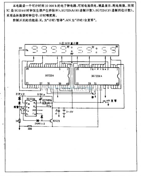
This circuit is electronic clock circuit. It can time to 10000h. It is supplied bybattery for liquid crystal display. Its power consumption is very small. The used IC is 5G5544 (clock generator generates pulse per second) , 5G7224A (60 system counting) , 5G7224 ( 10 system four digit counting) . The circuit uses crystal oscillation clock signal. Its time precision is high.
The function of control switch is: K2 is time/ suspend , AN is time/ all zero reset .
(View)
View full Circuit Diagram | Comments | Reading(1366)
DHY29-[48]24/10 type DC-DC converter principle diagram
Published:2011/12/4 22:04:00 Author:May | Keyword: DC-DC converter
![DHY29-[48]24/10 type DC-DC converter principle diagram](/uploadfile/ic-circuit/s2011410204646624.jpg)
At present, most communication equipments arealready unified and standard to use 48V DC power supply. But there are also few equipments continue using 24V DC power supply. Because the needed capacity of current is small, if we use rectifier toprovide power, for the purpose of guarantee incessant energy supply, we must use 24V accumulator battery. It is clear that it is not economy and occupation the space of equipment room. The suitable method to solve this problem is adopting 48V to 24V DC-DC converter. The diagram is DHY29-[48]24/10 type DC-DC converter principle diagram, its main performance index:
(1) input DC voltage nominal value: 48V permit change range: 41V~51V
(2) output DC voltage nominal value: 24V/10A permit change range: 21.6V~26.4V
(3) precision of voltage regulation: ≤±1%
(4) noise voltage phone balance weight noise voltage: ≤2mV, broadband noise voltage: ≤20mV (3.4kHz~30kHz) , peak to peak value noise voltage: ≤100mV, discrete frequency: ≤5mV (3.4kHz~150kHz) ≤3mV (150kHz~200kHz) ≤2mV (200kHz~500kHz) ≤1mV (0.5MHz~30MHz)
(5) efficiency: ≥80%
(6) Over voltage, under voltage, over current protection point and cut-off current. Over current: (29±1) V, under voltage: (21±1)V, over current: (12±1)V, cut-off current:10.5A~11A
(7) The current equalization of parallel operation: ≤±5% (View)
View full Circuit Diagram | Comments | Reading(1339)
Two normal shock converter circuit principle diagram
Published:2011/12/4 21:49:00 Author:May | Keyword: Two normal shock, converter
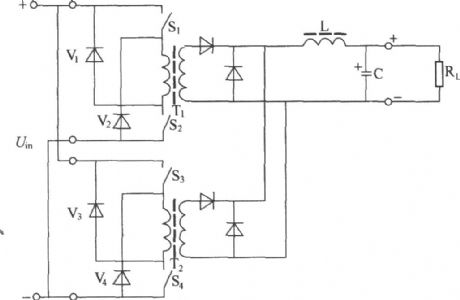
When it needs high output power, we always adopts two transistors forward converter circuit with superimposed voltage, and it isshown in the diagram. The features of the circuit:
(1)two normal shock converting circuits are connected inparallel, T1 and T2 are driven in 180opposite phase, then the power increases one time, and output frequency adds one time, ripples and dynamic responseare improving;
(2) S1, S2 are connected in series (S3, S4 are connected in series) , then the pressure-proof of switching tube is decreasd inhalve;
(3)The circuit cancels feedback coils, V1, V2, VpV4are energy recovery routes, it decreases the request of transformer’s manufacture craft.
(4)It hasthedead area limiting feature, two parts do nothave the problem of common circulation, its reliability is high. (View)
View full Circuit Diagram | Comments | Reading(1386)
Low resistance power distribution circuit
Published:2011/4/11 2:18:00 Author:may | Keyword: Low resistance, power distribution
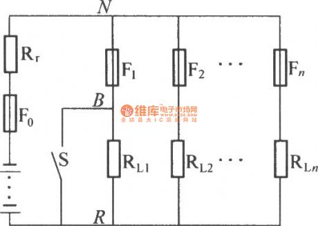
The diagram is low resistance power distribution circuit, among, R is battery internal resistance, RL1~RLn is load of each branch path; F1~Fn is safety wire of each branch path; F0 is battery safety wire, up and down two bold lines state total cylinder manifold.
Switch S short circuit, namely suppose if RL1 is short circuit, then before F1 burn out, at this time because battery internal resistance is more than F1 resistance, the voltage between N, R will drop to very low voltage, at the same time, because at this time the circuit in loop is basically depends on battery voltage and battery internal resistance, so short circuit current is enormous. When F1 burn out, because short current is high before F1 burn out, current change rate di/dt is also big, inductive kick LXdi/dt generated in equivalent inductance between N, R two points will form tremendous peak. At this time, voltage between N, R will first drop to zero in a moment, then generate a peak high voltage. These will have influenceon other branch path in the whole system which is abutting joint to one cylinder manifold. When low resistance power distribution, each branch load is not complete independence, and adopting multi-branch is go against of effective increase reliability of communications system. (View)
View full Circuit Diagram | Comments | Reading(1198)
Switching rectifier basic structure block diagram
Published:2011/4/11 2:07:00 Author:may | Keyword: Switching rectifier, basic structure

Switching rectifier mainly consists of four parts: input circuit, power inverter, rectifying and wave-filtering circuit and control circuit, as shown in the diagram. Input circuit makes AC input voltage rectifying and wave-filtering more flat high voltage DC voltage. Then the AC input voltagepass power inverter and change it to high frequency pulse voltage, thenpass rectifying and wave-filtering circuit change the high frequency pulse voltage to steady DC voltage, then output to load. The function of control circuit is to guarantee the stabilisation and adjustable of output DC voltage. (View)
View full Circuit Diagram | Comments | Reading(1534)
Single end normal shock converter circuit principle diagram
Published:2011/4/11 2:12:00 Author:may | Keyword: Single end, normal shock, converter
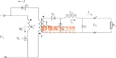
As shown in the diagram, when switch tube V1 is turn-on, input voltage Uin totally adds to justified of converter primary coil W1', induction voltage generates in degaussing iron ring W1'' make diode V2 cut-off, and induction voltage in secondary coil W2 make V3 turn-on, and sent the power of input current to inductance L0 and capacitance C and load; meanwhile it build up magnetizing current in converter, when V1 cut-off, V3 cut-ff, voltage direction on L0 is rollback andpass diode V4 to power supply to load continued, the magnetizing current in transformer willpass W1'', V 2 to release to input power source Uin and demagnetization; W1 has the function of clamp, the voltage on it is equivalent to input voltage Uin, before V1 turn- on again, demagnetizing current on T must release to zero, namely magnetic flux in T must reset, otherwise, transformer T will saturation and lead to the damage of V1. Normally, W1'=W1'', duty ratio of using two wires parallel winding coupled modes is <0.5, otherwise T will saturation. The wave form of single end normal shock converter is shown in the following diagram.
(View)
View full Circuit Diagram | Comments | Reading(1109)
Forward converter consists of two RC circuit
Published:2011/11/10 2:05:00 Author:May | Keyword: Forward converter , two RC circuits

View full Circuit Diagram | Comments | Reading(999)
The structure diagram of LDl001
Published:2011/11/10 2:06:00 Author:May | Keyword: structure
Because the frequency and duty factor changing of PWM signal is much larger, it can not convey simply through transformer.So SCALEis equipped with LDI001 logic drive interface. (View)
View full Circuit Diagram | Comments | Reading(1241)
Humidity indicator circuit
Published:2011/11/23 2:10:00 Author:May | Keyword: Humidity indicator
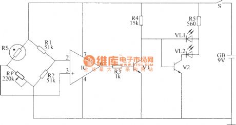
For the purpose of raising early and better seeding, in the village, people always use plastic film to make up simple raise seed shed in the ground. The disadvantage of this shed is the humidity in the shed is often too large, and it affects the normal growth of seeds. This example describes a simple seedling shed moisture indicator, which uses LED to indicate the size of the humidity of the greenhouse seedlings, and it is easy to use. This humidity indicator circuit consists of moisture detection amplifier and LED indication circuit, and it isshown in the diagram.
You can set the desired humidity alert by adjusting the resistance of RP.
Component selection:
R1 ~ R5 use 1/4W carbon film resistor or metal film resistors;
RP is organic, solid potentiometer or variable resistor. RS is made by 3DG6 transistors with the value greater than 100.
VL1 and VL2 choose light-emitting diodes φ5mm. V1 and V2 select 3DG6 or S9013 silicon NPN transistor. IC chooses μA741 or 5G24-type IC op amp IC. GB chooses 9V laminated battery. S chooses small single pole toggle switch. (View)
View full Circuit Diagram | Comments | Reading(1539)
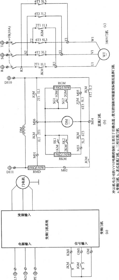
Beijing chongyun elevator door driver circuit
Published:2011/8/24 2:58:00 Author:Jessie | Keyword: Beijing chongyun , elevator door driver
View full Circuit Diagram | Comments | Reading(1336)
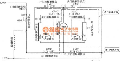
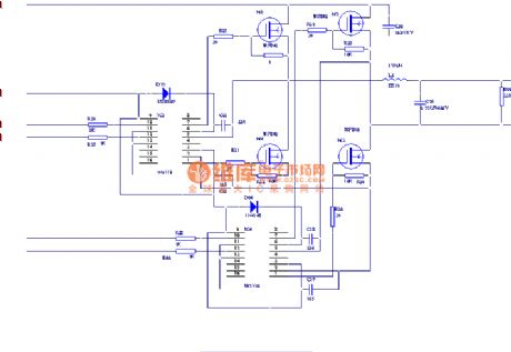
Beijing tujie Elevator door driver circuit
Published:2011/8/24 2:57:00 Author:Jessie | Keyword: Beijing tujie , Elevator door driver
View full Circuit Diagram | Comments | Reading(1223)
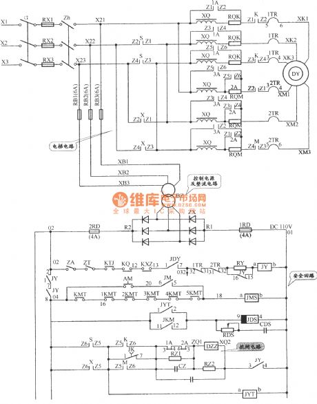
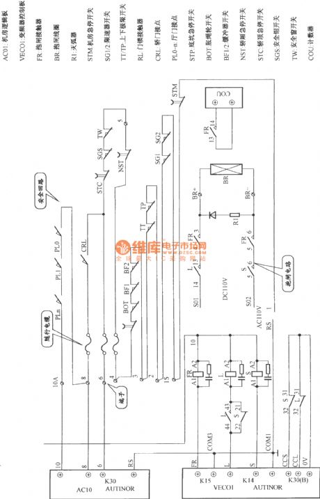
APM-81 The main circuit of elevator, safety loop and dlectrical circuit
Published:2011/8/26 4:06:00 Author:Jessie | Keyword: elevator, safety loop, dlectrical
View full Circuit Diagram | Comments | Reading(2496)
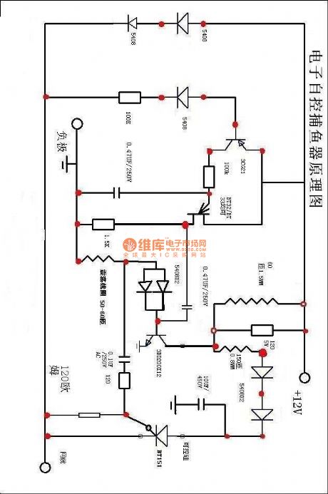
Fishing device 1
Published:2011/11/22 1:45:00 Author:May | Keyword: Fishing device
View full Circuit Diagram | Comments | Reading(2210)
Fishing Device
Published:2011/11/22 1:38:00 Author:May | Keyword: Fishing Device
View full Circuit Diagram | Comments | Reading(2327)
Beijing fuerrui elevator safety loop and band-type brake circuit
Published:2011/8/24 2:46:00 Author:Jessie | Keyword: Beijing fuerrui , elevator safety loop, band-type brake
View full Circuit Diagram | Comments | Reading(1188)
| Pages:7/126 1234567891011121314151617181920Under 20 |
Circuit Categories
power supply circuit
Amplifier Circuit
Basic Circuit
LED and Light Circuit
Sensor Circuit
Signal Processing
Electrical Equipment Circuit
Control Circuit
Remote Control Circuit
A/D-D/A Converter Circuit
Audio Circuit
Measuring and Test Circuit
Communication Circuit
Computer-Related Circuit
555 Circuit
Automotive Circuit
Repairing Circuit