
Electrical Equipment Circuit
Index 8
Boost and output practical circuit
Published:2011/11/22 0:42:00 Author:May | Keyword: Boost, output, practical

The diagram is a boost andoutput practical circuit. VT3 is switching regulating tube. Regulation tube VD2 can convert the potential. VT4 is paraphrase isolation amplifier. VT4 and its load which is 33kΩ resistor will divide the voltage Ui. The two voltages are separately provided to impulse generator. Impulse generator consists of transformer T and VT1, VT2. This is free running multi-vibrator of asymmetric transformer positive feedback. The power of VT1 comes from the voltage on 33kΩ resistor. The current on resistor depends on the current of VT4. The power supply voltage of VT1, VT2 is different. Each half period oscillation amplitude changes in direct proportion, the width changes in inverse proportion. Then it can control the turn-on and cut-off time. When output voltage is increasing, the current of differential pair tube VT6 of error amplifier is decreasing, collector potential is increasing, 33kΩ resistor up voltage drop is enlarge, VT1 tube power supply voltage is increasing, the turn on time is shortening, switching tube VT3’s turn on time is shortening.
The input voltage of this circuit is 12~28V, the output can be stabilized at 30V, the maximum output power is 60W, the efficiency is 88.9%~94.7%, the instability degree is ±0.33%, the output voltage ripple factor is 0.02&, the working frequency is 10kHz.
(View)
View full Circuit Diagram | Comments | Reading(1200)
The clamping single-end normal shock converter circuit with two transistors and diode
Published:2011/11/14 2:32:00 Author:May | Keyword: Two transistors , diode, clamping, single end, normal shock converter
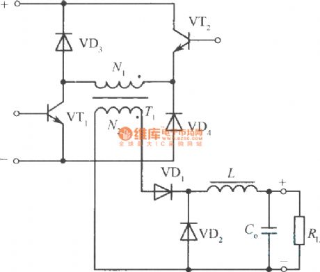
The following diagram is the clamping single-end normal shock converter circuit with two transistors and diode. VT1 and VT2are energized by PWM pulse and broken over and cut off at the same time. When they are cut off, polarity on N1 is reversing, diodes VD3 and VD4 are broken over, the potential is clamped. So, when VT1, VT2 are cut off, the voltage amplitude added between collectors are equal to input voltage Ui. (View)
View full Circuit Diagram | Comments | Reading(1212)
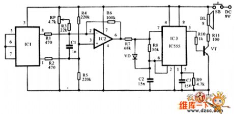
Phone minute beep decoder circuit with NE555, CD4017
Published:2011/8/30 2:09:00 Author:Jessie | Keyword: Phone minute beep, decoder
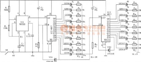
At present, our country telephone is executed with method of using minute as timing charging unit, except the charging in the first 1 min. Namely, the first time is fixed charging. Whenever enter the next time, the first 1s will immediately add the one-time charging. For the longer time's call speaking, the over 1 min should be paid low proportion in the whole conversation. But to those calls which often finished in the 1 min, even talk time delays 1 s, the over fee's proportion is high in the whole fee. The timing remind decoder circuit is shown as the chart. Full circuit is composed of the 6s time-base generator, 6s separate-frequency timing display and minute timing display. (View)
View full Circuit Diagram | Comments | Reading(4502)
Nianfeng YWQ-900 automatic electric pressure cooker circuit
Published:2011/8/24 2:16:00 Author:Jessie | Keyword: automatic electric pressure cooker
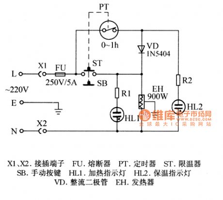
X1, X2-plug terminals, FU-fuse, PT-timer, ST-limit thermostat, SB-hand button, HL1-heating lamp, HL2-heat indicator, VD-rectifier diode, EH-heater (View)
View full Circuit Diagram | Comments | Reading(1834)
Gree ZGP series computer control electronic disinfection cabinet circuit
Published:2011/8/30 1:35:00 Author:Jessie | Keyword: Gree ZGP series , computer control, electronic disinfection cabinet
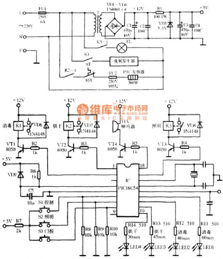
View full Circuit Diagram | Comments | Reading(916)
Light comparator circuit
Published:2011/11/24 1:11:00 Author:May | Keyword: Light comparator
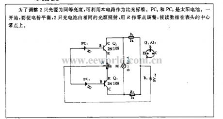
In order to adjust two light source to the same brightness, itcan use this circuit as light compare standard. PC1 and PC2are solar batteries. At the start, it should make the bridge keep balance, and the two photocellshas the same light source, and it uses R as zero adjustment to make the read number point at center zero of guage head.
(View)
View full Circuit Diagram | Comments | Reading(997)
Sickroom calling device circuit
Published:2011/11/30 21:14:00 Author:May | Keyword: Sickroom calling device
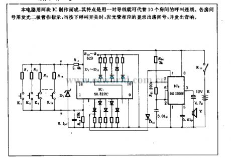
This circuit is composed of two ICs, its features are that it can use a pair of wires toreplace the calling wires in ten rooms. Every room number uses LED as indication, when people press calling switch, corresponding LED displaysroom number, and emits voice.
(View)
View full Circuit Diagram | Comments | Reading(1168)
Audio frequency therapeutic apparatus circuit
Published:2011/11/9 21:07:00 Author:May | Keyword: Audio frequency, therapeutic apparatus
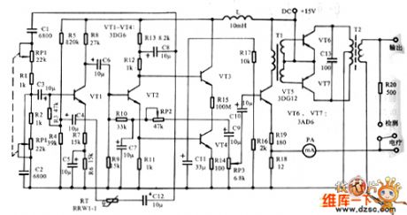
Audio frequency therapeutic apparatus circuit principle is shown in the diagram. It consists of RC oscillator, preamplifier, push-pull power amplifier and the output current indicator, etc. In fact, it is an audio frequency signal generator with high output power.
In the diagram, transistors VT1 and VT2and some resistor-capacitor unit, etc make up wien bridge oscillator with goodwaveform and widelow-frequency adjustable range.The double potentiometer RP1 can adjust oscillator frequency.
Transistors VT3 and VT4 make up the series push-pull amplifier of non output transformer. VT3 and VT4are two transistors with the same polarity, and theyuse series type, and two bases of the transistor areseparately connectedto the collector and emitter of VT2 in order to get oposite phase signal, thereby lt makes VT3 and VT4's bases add to the same amplitude, phase and oposite oscillator signal.
(View)
View full Circuit Diagram | Comments | Reading(1536)
Farm and sideline products autoregulation drying box circuit
Published:2011/11/23 21:41:00 Author:May | Keyword: autoregulation drying box
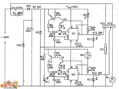
Circuit working principle:
This farm and sideline products autoregulation drying box circuit consists of power source circuit, temperature control circuit and humidity control circuit, is shown in the diagram.
Power source circuit consists of buck capacitor Cl, discharge resistors Rl, rectifier diodes VDl, VD2, filter capacitor C2, current limiting resistors R2, R3, zener diode VS, and power indicator LED VLl.
Temperature control circuit consitsts of thermistance RT ( temperature sensor) , time base intergrated circuit IC1, transistors V1, V2, resistors R4, R6-R8, R12, potentiometers RP1, RP3, capacitors C3, C5, LED VL2, thyristor VT1. At the same time, C3discharges byRP1, R8 and pin 7 of IC1 circuit , when C3 justified voltage decreases to about 3.3V, IC1 pin 3 will output high level to make V1, V2 and VT1 breakover, EH starts heating.
RI and R2 select 1/2W metal film resistors ; R3-R13 use 1/4W metal film resistor or carbon film resistors.RT uses MZ2A positive temperature coefficient thermistor .RS uses ZHC-l or MSO-1 humidity sensitive resistor device . (View)
View full Circuit Diagram | Comments | Reading(1590)
Y977A/B thunderbolt flash integrated module circuit
Published:2011/11/3 22:20:00 Author:May | Keyword: thunderbolt flash integrated module
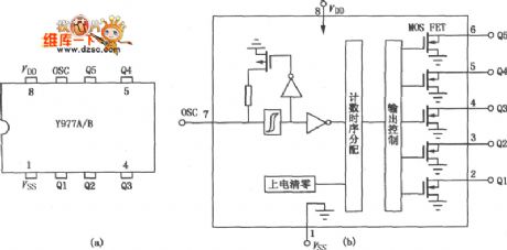
Y977A/B module can be applied to various household appliances forelectronic flashing control, such as tape recorders, audio flash show etc, it also can be used in theaters, discos and flash control store ornamental, electronic toys flashing and motorcycle trunk flashing control etc. The diagramshows its pin arrangement.
(View)
View full Circuit Diagram | Comments | Reading(1286)
Auto saving alarm working principle circuit
Published:2011/11/4 1:34:00 Author:May | Keyword: Auto saving alarm
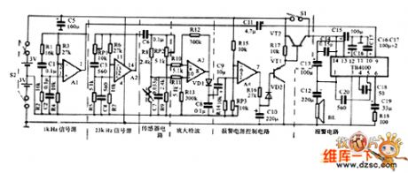
Working principle:
When people arewalkingor working,thebody will move more or less, when wearer is faint or totally stops movement, the saving alarm can auto emit sound call for help.
Saving alarm consisits of signal source, sensor circuit, amplifier, alarm power control circuit and sound alarm circuit. Circuit principle is shown in the first diagram. The four operational amplifiers A1, A2, A3, A4 in the circuitatr four operatational amplifiers. A1, A2 separately make up two wien bridge oscillators which isusedas signal source,and C11 and C6 are coupling to alarm and sensor circuit.
After human body stops move, sensor circuit bridge is in balance state, then the difference amplifier A3 has no fluctuation signal output, comparator A4 generates a steady +0.4V voltage. After comparator rollback, beacause R16, C10's delay effect, after 5s, C10 voltage drops to +3.5V, it makes voltage regulator diode 2CW9 breakover, the alarm circuit emits alarm signal.
Alarm circuit consist of sound integratedblock TB4100. The 1KHz sound frequency signal generated by A1, then it is coupled to TB4100 through capacitor C11.
(View)
View full Circuit Diagram | Comments | Reading(1122)
Touching eight-sound five-flash dynamic toy circuit diagram
Published:2011/11/4 1:53:00 Author:May | Keyword: Touching , eight-sound, five-flash, dynamic toy
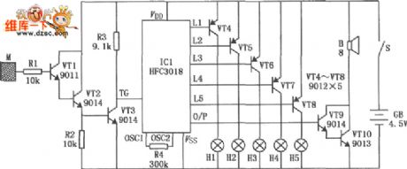
Touching eight-sound five-flash dynamic toy circuit diagram is shown in the diagram. It consists of HFC3018 module, and it can generate eight kinds ofdifferent voices: like step gunfire, aviation gunfire, game sight, telephone sight, bomb 1, bomb 2 sound, machine guns 1 sound and machine guns 2 sound, at the same time, itcan drive five small bulbs shining in an order.
(View)
View full Circuit Diagram | Comments | Reading(2860)
Low input current low power consumption peripheral driver circuit
Published:2011/11/9 20:21:00 Author:May | Keyword: Low input current , low power consumption, peripheral driver circuit
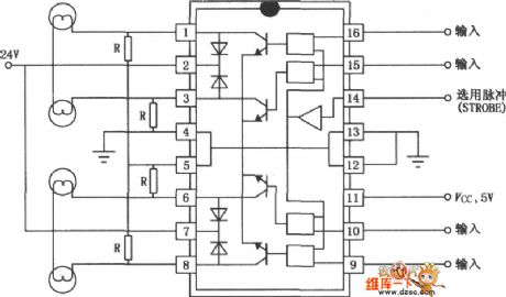
SN75436/75437A/75438 is low input current, low power consumption monolithic four-channel, OC, inverted output peripheral driver, which is used ashigh current, high voltage load driver. This chip's input current is low, power consumption islow, output voltage is high, output impedance ishigh,and it has theoutput clamping diode. The diagram is wiring diagramwhen it is usedas lamp driver.
(View)
View full Circuit Diagram | Comments | Reading(1072)
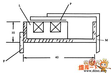
DC motor commutator circuit
Published:2011/11/3 1:58:00 Author:May | Keyword: DC motor commutator
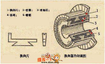
The important component of DC motor, and its functionis to transform the DC current to AC current in the coil ofelectric brush or transform the AC electromotive force to DC electromotive force.
diagram: DC moitor commutator circuit (View)
View full Circuit Diagram | Comments | Reading(2433)
The commutating pole circuit of DC motor
Published:2011/11/23 21:19:00 Author:May | Keyword: commutating pole , DC motor
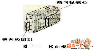
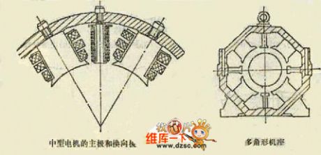
The schematic diagram of the main pole and the interpole (View)
View full Circuit Diagram | Comments | Reading(1321)
New degaussing principle circuit
Published:2011/11/11 2:03:00 Author:May | Keyword: degaussing principle
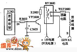
Because the voltage on capacitor C2605 can not mutation, this high level signal thorugh R2602 resistor first charges to C2605, because charging time constant is very big, the high level potential build at C2605 lags to the start time. Whenit isin starting process, capacitor finishes charging, VT2600 tube's base is inhigh level and breakover, relay RY2600 coil generates current access, its touching point is cut-off, degaussing circuit power source ( AC) accessis cut, thereby itfinishes the cut-off movement of degaussing circuit.
diagram 3: TV new type degaussing circuit
After shutdown, IC001's pin changes to low level, capacitor C2605discharges through VT2600's b-e junctions and IC001 internal concerning circuit, and the discharging time constant is also very high, so VT2600 tube changes to cutoff state after delay period of time, relay RY2600 again recovers to normal close state for degaussing next time.
(View)
View full Circuit Diagram | Comments | Reading(1565)
Blind electronic compass circuit
Published:2011/11/30 21:05:00 Author:May | Keyword: electronic compass
The core device IC1 of electronic compass is a piece of hall-effect integration sensor UGN-3501M, its internal structure includes a hall unit and a linear differential amplifier with differential emitter-follower output.
The circuit principle is shown in the diagram: the integrated hall sensor IC1 changes the earth's magnetic field to differential output voltage; this voltagepasses IC1's two output ends pin 8 adn pin 1 and resistors R1 and R2,then it is added toanother difference amplifier IC2 ( μA741) . When IC1 output is zero,RP is used to adjust the output voltage of IC2; capacitor C1 isused to suppress parasitic oscillation. R8, C2 , and VD (1N4148)are thecharge and discharge devices of time-base circuit. (View)
View full Circuit Diagram | Comments | Reading(2731)
Blind crowing device circuit
Published:2011/11/23 21:45:00 Author:May | Keyword: Blind crowing device
The blind always feel not convenientwhen they usetiming clock to crow herald the break of a day,so using blind crowing device circuit to make crowing device is very convenient.
Transistor VT1 is optical transistor, when it has different illumination, its resistance value changes comparatively large, integrated circuit IC1 (5G1555) makes up free-running multivibrator, its oscillator frequency rises along with the add of lumen output. The oscillator frequency and dutyfactor of oscillator depends on resistor R2, photoelectric cell VT1 (3DU22) and capacitor C1. Resistor R2 ensures the upper limit frequency at about 6.5KHz. Photoduodiode VT1's dark resistor makes lower limit frequency fix at about 1Hz.
Sound relationship with the Sky output as follows:
Sky output/ VT1 resistor/ frequency
sunshine enough/100Ω/6500Hz
evening/ 10K/3000Hz
starlight/ 10M/ 2~4Hz
(View)
View full Circuit Diagram | Comments | Reading(992)
Electronic biological wave physiatrics instrument circuit
Published:2011/10/31 4:02:00 Author:May | Keyword: Electronic biological wave, physiatrics instrument
Electronic biological wave physical physiatrics instrument is shown in the following diagram, it can generate the compoundsignal with various frequency, and it canhelp patients absorb medications,and italso hasdirect effect on the human body acupuncture point for treatment.
(View)
View full Circuit Diagram | Comments | Reading(2381)
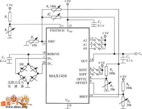
Pressure signal conditioning circuit composed of MAX1450
Published:2011/10/31 1:24:00 Author:May | Keyword: Pressure signal conditioning
View full Circuit Diagram | Comments | Reading(1118)
| Pages:8/126 1234567891011121314151617181920Under 20 |
Circuit Categories
power supply circuit
Amplifier Circuit
Basic Circuit
LED and Light Circuit
Sensor Circuit
Signal Processing
Electrical Equipment Circuit
Control Circuit
Remote Control Circuit
A/D-D/A Converter Circuit
Audio Circuit
Measuring and Test Circuit
Communication Circuit
Computer-Related Circuit
555 Circuit
Automotive Circuit
Repairing Circuit