
Electrical Equipment Circuit
Index 17
Visitors identifying electronic doorbell
Published:2011/8/11 20:13:00 Author:Ecco | Keyword: Visitors identifying, electronic doorbell
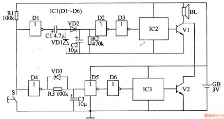
The electronic doorbell circuit is composed of the short pulse identification circuit, long pulse identification circuit and circuit music generating circuit, amd it is shown in Figure 3-120. Short pulse identification circuit consists of the NOT gates D1-D3 which are inside of the six NOT gate integrated circuit ICl, resistors C1, C2 and diodes VD2, VDl. Long pulse identification circuit consists of the NOT gates D4-D6 which are inside of the ICl, resistor R3, diode VD3 and capacitor C3. Music generating circuit consists of the music integrated circuits IC2, 1C3, audio amplification tube Vl and V2, speaker BL and so on. S is the doorbell button. R1 is the current limiting resistor.
(View)
View full Circuit Diagram | Comments | Reading(1319)
Percussion electronic doorbell 2
Published:2011/8/11 21:33:00 Author:Ecco | Keyword: Percussion electronic doorbell
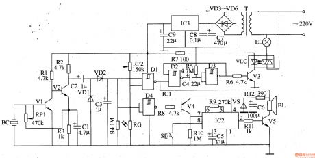
The percussion electronic doorbell circuit is composed of the percussion detection circuit, voltage doubling rectifying circuit, lamp trigger delay control circuit, light control circuit, doorbell trigger circuit, audio circuit and power supply circuit, and it is shown in Figure 3-114. Percussion detection circuit consists of piezoelectric ceramic BC, amplification tubes Vl and V2 and external RC components. Voltage doubling rectifying circuit is composed of the rectifier diodes VDl and VD2, capacitor C3 and other components. Lamp trigger delay control circuit consists of the internal triggers D1-D3 of four NAND gate Schmitt trigger circuit ICl, transistor V3, light coupler VLC and peripheral RC components.
(View)
View full Circuit Diagram | Comments | Reading(1418)
Percussion electronic doorbell 1
Published:2011/8/11 21:21:00 Author:Ecco | Keyword: Percussion electronic doorbell
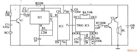
The electronic doorbell circuit is composed of the pickup amplifier, monostable trigger circuit, pulse counter circuit, music generating circuit and audio amplifier circuit and other components, and it is shown in Figure 3-113. Pickup amplifier circuit consists of piezoelectric ceramic BC, amplification tube Vl, resistors Rl and R2 and capacitor Cl and so on. Monostable trigger circuit is composed of the D flip-flop which is inside of the dual D flip-flop IC and the external components. Pulse counter circuit is composed of decimal pulse counter integrated circuit IC2. Music generating circuit is composed of the music IC IC3 and the external RC components.
(View)
View full Circuit Diagram | Comments | Reading(2560)
Boiler electronic descaling device circuit diagram 4
Published:2011/8/21 21:55:00 Author:Ecco | Keyword: Boiler , electronic descaling device
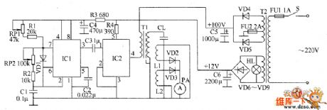
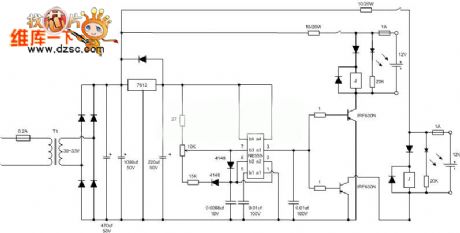
The boiler electronic descaling device circuit is composed of the power supply circuit, 200kHz square wave oscillator, driver amplifier and the output indication circuit, and it is shown as the chart. Power supply circuit is composed of the power transformer T2, rectifier diodes VD4 ~ VD9, filter capacitors C5, C6 and so on. 200kHz square wave oscillator circuit is composed of the time-base integrated circuit IC1 and the external components. Driver amplifier circuit is composed of the high-power electronic switching amplifier IC IC2, output transformer T1 and the capacitive load CL and so on. Output indication circuit is composed of the current meter PA, rectifier diodes VD2, VD3 and current mutual inductance coils L1, L2 and so on.
(View)
View full Circuit Diagram | Comments | Reading(5154)
Battery restorer schematic diagram
Published:2011/8/24 2:06:00 Author:Ecco | Keyword: Battery restorer
View full Circuit Diagram | Comments | Reading(1368)
Micro-programmer circuit diagram
Published:2011/8/25 1:20:00 Author:Ecco | Keyword: Micro-programmer
View full Circuit Diagram | Comments | Reading(2635)
Konka bt580 rear projection TV line scanning and video processing circuit diagram
Published:2011/8/25 1:54:00 Author:Ecco | Keyword: Konka , rear projection TV , line scanning , video processing
View full Circuit Diagram | Comments | Reading(2580)
Transistor Arithmetic Product Wave Detector Circuit
Published:2011/8/23 23:41:00 Author:Robert | Keyword: Transistor, Arithmetic, Product, Wave, Detector
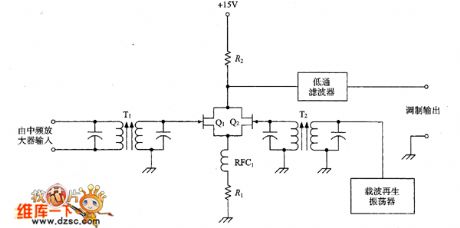
The picture shows the arithmetic product wave detector circuit composed of dual-electrode transistor. The action of the circuit likes a amplifier. But the base electrode of the transistor is controlled by the local oscillator. The SSB signal would input from the T1's low-impedance secondary coil and then it should be normally amplified by Q1. But the local oscillator inhibiting action stop this process. The local oscillator controls the transistor connected or disconnected. It produces the nonlinear feature needed by demodulation.
The picture shows the transistor arithmetic product wave detector circuit. (View)
View full Circuit Diagram | Comments | Reading(1019)
Dual JFET Arithmetic Product Wave Detector Circuit
Published:2011/8/23 23:41:00 Author:Robert | Keyword: Dual, JFET, Arithmetic, Product, Wave, Detector
In the picture, it uses a couple of differencial signal junction type FET (JFET) to generate the arithmetic product wave detection. The SSB signal is added to the Q1's grid electrode. The local oscillator is used to interrupt the circuit in the Q2 side. It should note that the local oscillator's signal amplitude is much stronger than the SSB signal. The two tubes' common drain electrode circuit is connected to a low-pass filter and then it connects the output port. The filter is adjusted to the spectra which is needed to be overlayed (usually it is the audio frequency).
The picture shows the dual JFET arithmetic product wave detector circuit. (View)
View full Circuit Diagram | Comments | Reading(1485)
MOSFET Arithmetic Product Wave Detector Circuit
Published:2011/8/23 23:41:00 Author:Robert | Keyword: MOSFET, Arithmetic, Product, Wave, Detector
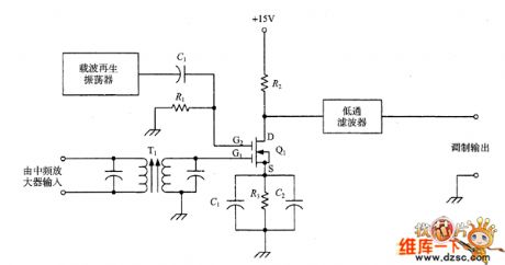
The circuit shown in the picture a MOSFET with dual grid electrodes: the G1's normal signal input is used to receive the SSB signal from the IF amplifier; the G2's local oscillator signal would control the MOSFET's switch. The audio low-pass filter is also in the output (drain electrode) circuit to limit the redundant IF signal from the demodulator output.The picture shows the MOSFET arithmetic product wave detector circuit.Notes: in this circuit the MOSFET's source circuit has two capacitance (C1 and C2). Typically one is RF capacitance and the other is AF capacitance. Although using the modern capacitors, this distinction is not very necessary. (View)
View full Circuit Diagram | Comments | Reading(1063)
MC-1496 Arithmetic Product Wave Detector Circuit
Published:2011/8/23 23:41:00 Author:Robert | Keyword: Arithmetic, Product, Wave, Detector
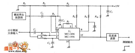
The picture shows a integrated SSB arithmetic product wave detector circuit. The circuit is based on the MC-1496 analog multiplier chip. It contains a transconductance unit demodulator whose switch is controlled by a local oscillator. The SSB mid-frequency signal would input to the pin 1 and the local oscillator would input to the pin 10. Other pins would be added the corresponding bias voltage according to different working conditions or not used.
The picture shows the MC-1496 arithmetic product wave detector circuit. (View)
View full Circuit Diagram | Comments | Reading(2577)
Dual Tuning Frequency Detector Circuit
Published:2011/8/23 23:41:00 Author:Robert | Keyword: Dual, Tuning, Frequency, Detector
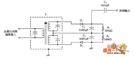
A classic FM frequency detector circuit is shown in the picture. The circuit uses a special transformer which has two secondary windings. The two secondary windings are separately connected to the two sides of the IF frequency which have the same distance to IF frequency and are not fay from the IF frequency. The two frequency's distance should be a little bigger than the transmitter's amplitude. The output would combine through a couple differencial signal diodes (D1 and D2). The diodes' output ports are connected to the load resistor R1 and R2. Generally, when the signal has not been modulated, the algebraic sum of the two diodes' output is zero. That would make the output be zero. (View)
View full Circuit Diagram | Comments | Reading(1054)
PNP Output Regulator Grounding Current Circuit
Published:2011/8/23 23:39:00 Author:Robert | Keyword: PNP, Output, Regulator, Grounding, Current
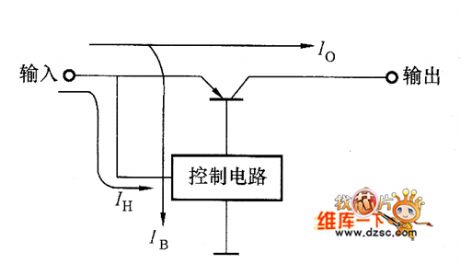
The PNP output low-voltage-drop regulators' common weakness is the grounding current (current consumption of the regulator itself) is more than the input current. Also the output current causes the grounding current having a big variation. The PNP output regulator is that the transistor's base electrode current control the load current, thus this base electrode current would go through the ground and make up a part of the grounding current. As shown in the picture, thepicture shows the control circuit consumption current, also the picture shows the base current. The IH is output current. So, even the load current (the transistor collector electrode current) is small, the I/hFE's grounding current would also change to be the consumption current. (View)
View full Circuit Diagram | Comments | Reading(1261)
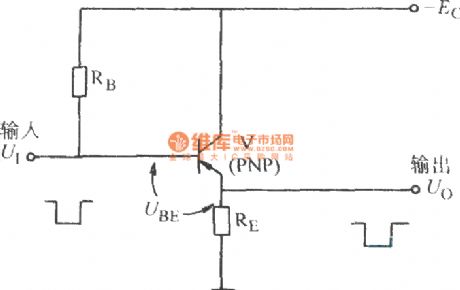
Emitter follower circuit
Published:2011/8/23 2:06:00 Author:Ecco | Keyword: Emitter follower
View full Circuit Diagram | Comments | Reading(1395)
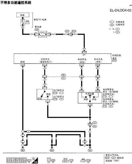
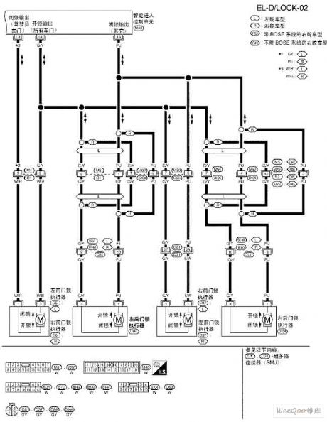
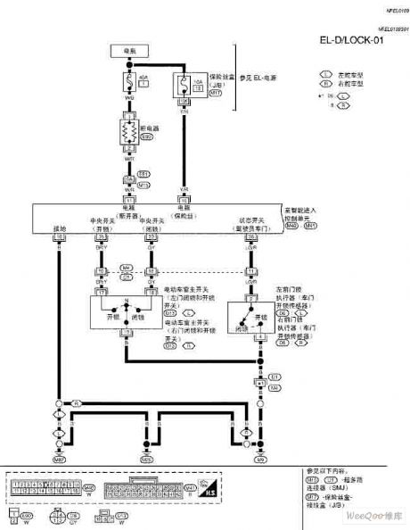
Teana A33-EL electric door lock circuit diagram 3
Published:2011/8/12 3:24:00 Author:Lucas | Keyword: Teana, electric door lock
View full Circuit Diagram | Comments | Reading(907)
Teana A33-EL electric door lock circuit diagram 2
Published:2011/8/12 3:24:00 Author:Lucas | Keyword: Teana , electric door lock
View full Circuit Diagram | Comments | Reading(1076)
Teana A33-EL electric door lock circuit diagram 1
Published:2011/8/12 3:25:00 Author:Lucas | Keyword: Teana , electric door lock
View full Circuit Diagram | Comments | Reading(1073)
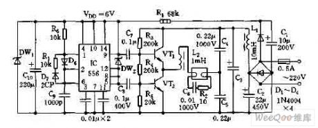
Electronic ballast circuit diagram
Published:2011/8/12 3:22:00 Author:Lucas | Keyword: Electronic ballast
View full Circuit Diagram | Comments | Reading(1499)
Double-digit display seconds timer circuit diagram
Published:2011/8/11 2:23:00 Author:Rebekka | Keyword: Double-digit display , seconds timer
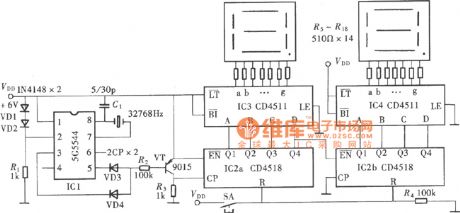
Double-digit display seconds timer(5G5544、CD4511、CD4518) circuit diagram is shown as above.
The maximum time timer of explicit two-digit seconds is 99s. The circuit is composed of a time-base signal which is quartz clock IC 5G5544 output pulse signal. Since the pulse period of circuit output is 2s, it achieves the seconds output functionby matchingwith transistor VT and two input ends of the counter. (View)
View full Circuit Diagram | Comments | Reading(3434)
The application circuit of driving 5 white light LEDs
Published:2011/8/18 3:40:00 Author: | Keyword: application circuit, white light LEDs
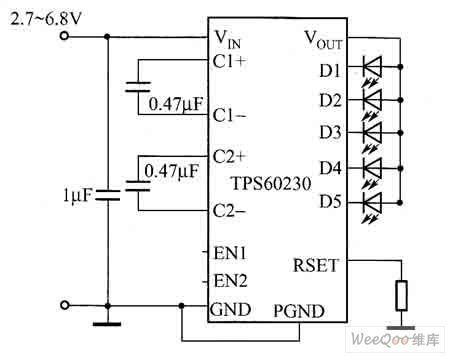
TPS60230 can drive 5 25mA white light LEDs at most; TPS60231 can drive 3 25mA white light LEDs at most; the main technology features of TPS60230/TPS60231 are shown as follows.①the brightness of the white light LED can be controlled by PWM; ②it has the 1 and 1.5 time shift modes of self-adaption, and it can get high efficiency; ③the shift frequency is 1MHz; ④the working input voltage range is 2.7~6.5V; ⑤it contains the soft starting circuit, by which the transient state influx current can be impeded; ⑥low input wave and low EMI(electromagnetic disturbance).
(View)
View full Circuit Diagram | Comments | Reading(1069)
| Pages:17/126 1234567891011121314151617181920Under 20 |
Circuit Categories
power supply circuit
Amplifier Circuit
Basic Circuit
LED and Light Circuit
Sensor Circuit
Signal Processing
Electrical Equipment Circuit
Control Circuit
Remote Control Circuit
A/D-D/A Converter Circuit
Audio Circuit
Measuring and Test Circuit
Communication Circuit
Computer-Related Circuit
555 Circuit
Automotive Circuit
Repairing Circuit