
Circuit Diagram
Index 2037
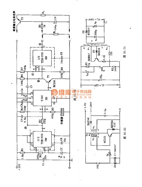
Microprocessor electric typewriter circuit
Published:2011/4/21 4:23:00 Author:Nicole | Keyword: microprocessor, electric typewriter
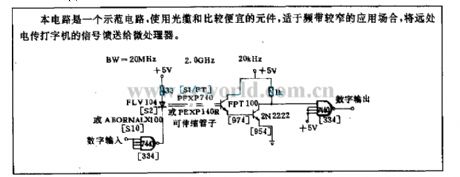
This circuit is a model circuit, it adopts fiber optic cable and some cheaper components and it is used in the occasions with narrow frequency band, it feeds the microprocessor with singal of forane electric typewriter. (View)
View full Circuit Diagram | Comments | Reading(716)
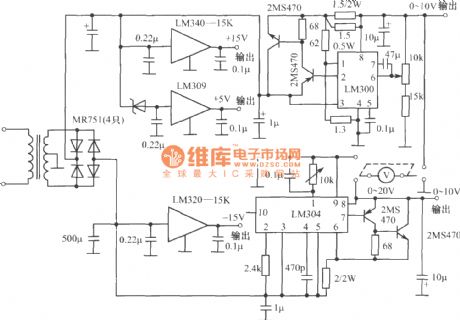
Common regulated power supply
Published:2011/4/21 4:37:00 Author:Nicole | Keyword: regulated power supply
View full Circuit Diagram | Comments | Reading(689)
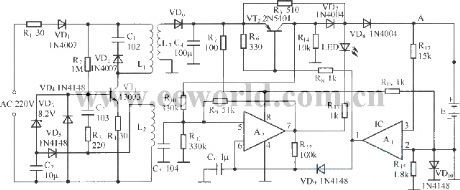
Common mobile phone battery charger circuit BQ2057
Published:2011/4/21 4:39:00 Author:Nicole | Keyword: mobile phone battery, charger
View full Circuit Diagram | Comments | Reading(1626)
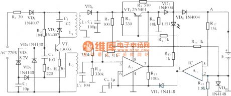
Common mobile phone battery charger circuit(BQ2057)
Published:2011/4/21 4:40:00 Author:Nicole | Keyword: mobile phone battery, charger
View full Circuit Diagram | Comments | Reading(2027)
Colour TV power supply controller circuit
Published:2011/3/30 1:28:00 Author:may | Keyword: Colour TV power supply controller
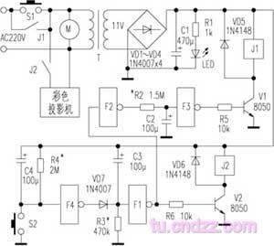
View full Circuit Diagram | Comments | Reading(1605)
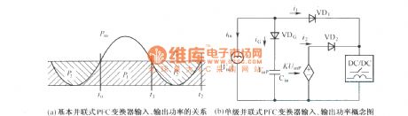
Relationship of multiple system PFC convertor input, output power
Published:2011/3/30 22:00:00 Author:may | Keyword: multiple system, PFC convertor
View full Circuit Diagram | Comments | Reading(529)
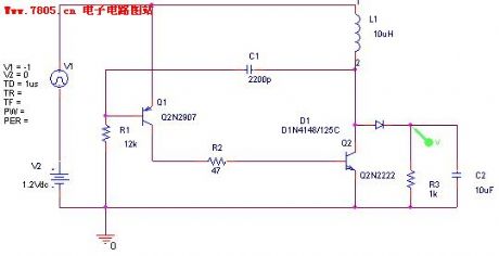
Simple and practical boosted circuit
Published:2011/4/20 20:58:00 Author:May | Keyword: Simple and practical, boosted
View full Circuit Diagram | Comments | Reading(500)
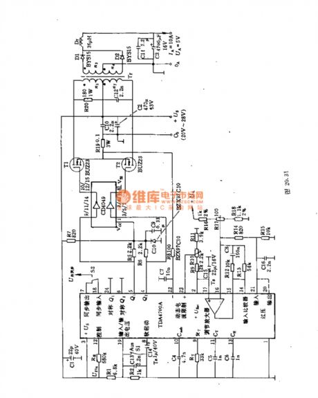
50W DC voltage converter using SIPMOS power transistor and integrated circuit
Published:2011/4/20 21:22:00 Author:May | Keyword: 50W, DC voltage converter, SIPMOS power transistor, integrated
This circuit adopts push pull type DC converter of integrated circuit TDA4700. Its input voltage is 20~28V. Its output voltage is 5V. The maximum load current is 10A. The oscillation frequency of integrated circuit is 40kHz.
Technical data: (1)input voltage Ui:min=20V, typ=24V, max=28V; (2)output voltage Uo: typ=5V; (3)output current Io: min=0A, max=10A;(4)load adjustment rate (load step change 30~100%) : typ=0.2%; (5)efficiency η: typ=81%; (6)SIPMOS transistor loss: when breaking over, PVD: typ=1W; when opening and closing PVS: typ=0.4W; total loss: PVD+PVS: typ=1.4W.
Transformer data: n1=n2=14turns, double wrap, twisted wire 120×0.1mm copper enamel wire;
n3=n4=5turns, double wrap, twisted wire 120×0.1mm copper enamel wire. (View)
View full Circuit Diagram | Comments | Reading(464)
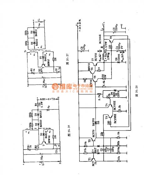
5V~24V/5A adjustable DC voltage converter with current limitting
Published:2011/4/20 21:39:00 Author:May | Keyword: 5V~24V/5A, adjustable, DC voltage converter, current limitting
This circuit adopts three spread fast power transistors BUY55 and fast power diode SSiE3055 as switching component. The control frequency is 20kHz and is out of hearing frequency range. Power supply by 24V storage battery, this circuit can change it to TTL circuit used 5V power supply. It is used in automobile or other industrial circle. Its efficiency is higher than 70%.
Main technical data:
Working voltage: 24±25%V;
Oscillation frequency: ≈20kHz;
Output voltage: 5V (3~6V);
Maximum output noise voltage: 20mV (peak to peak value);
Maximum output current: 5A;
Minimum output current: 0.3A;
Current limiting value: ≈5.5A;
Regulation factor: 0.04. (View)
View full Circuit Diagram | Comments | Reading(500)
5V-+12V and -15V DC converter
Published:2011/4/20 22:00:00 Author:May | Keyword: 5V-+12V and -15V, DC converter
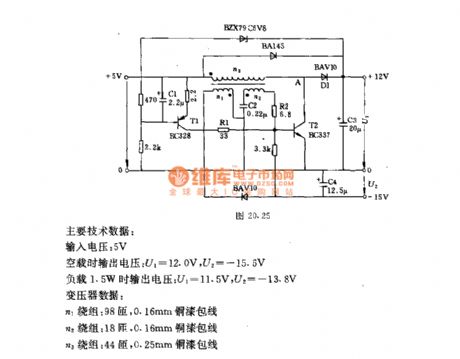
When this circuit is in stable state, capacitor C3 has about 12V voltage, transistor is breaking over, its collector potential is only few tenths of millivolt. So D1 is blocked off. The currents flow to load through transformer secondary winding and transistor T2. Output voltage is feeding back to the base of T1 through BZX79C6V8. The changing of output voltage leads to the change of collector current. And output voltage is stable by the changing of square wave's duty factor.
Main technical data:
Input voltage: 5V;
output voltage when non load: U1=12.0V, U2=-15.6V;
Output voltage when the load is 1.5W: U1=11.5V, U2=-13.8V.
Transformer data:
n1 winding: 98turns, 0.16mm copper enamel wire;
n2 winding: 18turns, 0.16mm copper enamel wire;
n3 winding: 44turns, 0.25mm copper enamel wire.
(View)
View full Circuit Diagram | Comments | Reading(2210)
80V-12V/10A DC voltage converter
Published:2011/4/20 22:08:00 Author:May | Keyword: 80V-12V/10A, DC, voltage converter
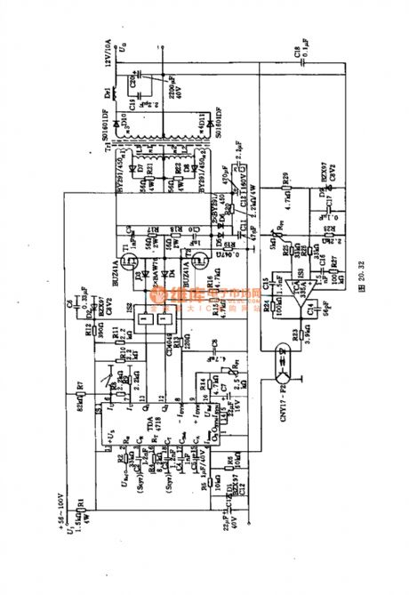
This push pull type converter adopts two SIPMOS transistors BU41A and a piece of integrated circuit TDA4718 as naval vessel network power supply. The input side and output side of converter is isolation. Its working frequency is 50kHz. Its efficiency is 75%. The power supply voltage can change in the range of 56~100V. The output changes to 12V by transformer, then it will pass full wave rectifier of D10, D11, finally, it will smooth to DC by output filter Dr1, C20 and C19.
(View)
View full Circuit Diagram | Comments | Reading(2389)
6V-12V/25W DC voltage converter
Published:2011/4/20 22:17:00 Author:May | Keyword: 6V-12V/25W DC voltage converter
It can adopt single side breaking over converter for low voltage and high power output converter. The oscillation frequency is chose 250Hz in order to decrease the changing loss of transistor AD133.
Main technical data:
Working voltage: 6V (maximum is 8.3V);
Working current: 10A;
Output voltage: 12V;
Output power: 28W;
Efficiency: 46%;
Oscillation frequency: 250Hz.
Transformer data:
n1=20turns, 4×1.0mm copper enamel wire;
n2=40turns, 2×1.0mm copper enamel wire;
n3=8turns, 1.0mm copper enamel wire.
(View)
View full Circuit Diagram | Comments | Reading(2102)
tda2030 btl amplifier circuit diagram
Published:2011/3/30 22:00:00 Author:Ecco | Keyword: amplifier
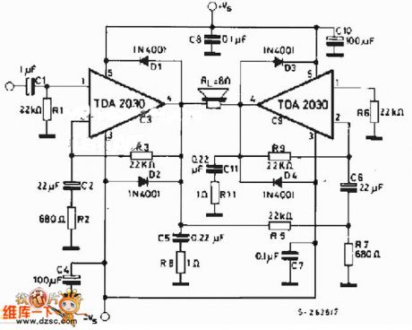
tda2030 btl amplifier circuit diagram is as below. The power amplifier of BTL, its main featuresare under the same power supply voltage and the load resistance condition, it can receive higher output power than OCL or OTL circuits.
(View)
View full Circuit Diagram | Comments | Reading(10842)
Infrared reflector type of electronic bell circuit diagram
Published:2011/3/30 22:55:00 Author:Ecco | Keyword: Infrared reflector type , electronic bell
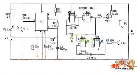
The infrared reflector type of electronic bell, can transmit voice frequency semaphore to tell host that vistors are coming in definite distance. The bell is also a type of annunciator. The working principle is that infrared reflector type of electronic bell consisting of infrared emission circuitry, infrared receive circuitry, low frequency oscillator, audio oscillator, audio output circuitry. etc. According to the chart:
(View)
View full Circuit Diagram | Comments | Reading(1279)
Clairaudit audiphone circuit diagram
Published:2011/3/30 22:21:00 Author:Ecco | Keyword: Clairaudit audiphone
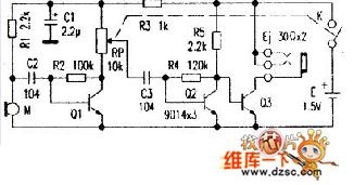
The Clairaudit audiphone is composed of discrete component with simple structure and small volume. The circuit diagram is decided according the material object, it's provided forreference while coping now.
In the figure, microphone could receive aural signal. Q1 and Q2 make up second order audio amplifier. As power amplifier, Q3 amplifies the aural signalandlistened by stereophone, and Rp can rectify the volume. Under normal working circumstance, the voltage of Q1, Q2 is 0.5V, and the quiescent current is 10mA. When the voltage falls to 1.1 V, the sound in the earphone is still clear. (View)
View full Circuit Diagram | Comments | Reading(614)
Shanghai GOL sedan circuit diagram
Published:2011/3/30 22:33:00 Author:Ecco | Keyword: GOL sedan
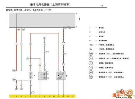
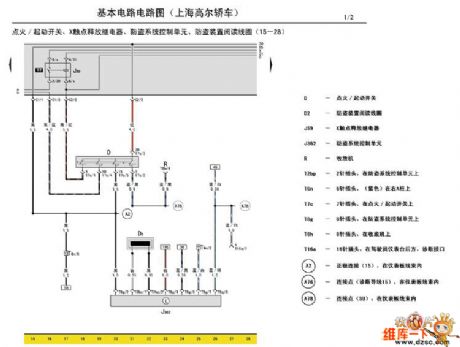
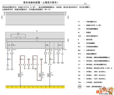
Shanghai GOL sedan circuit diagram is as below:
(View)
View full Circuit Diagram | Comments | Reading(531)
Dong Feng EQ1090 circuit diagram
Published:2011/3/30 22:56:00 Author:Ecco | Keyword: Dong Feng
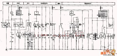
Dong Feng EQ1090 circuit diagram is as below:
1-front sidemarker; 2-grouped lamps; 3-headlamp; 4-ignition co-il; 4 n-additional resistanc wire; 5-distributor; 6-sparking plug; 7-alternator; 8-alternator modulator; 9-speaker; 10-work lamp socket; 11-speaker relay; 12-genial breezes motor; 15-water temperature sensor machine; 16-lamp optical relay; 17 a-d-fuses; 18-blinker; 20-lamp switch; 22- left or right direction indicator; 23- low oil pressure warning light; 25- optics switch; 26-start machine; 27-the oil pressure gauge sensor; 28-low oil pressure warning switch; 29-secondary cell; 30-power supply master switch; 31-the start reunite relay; 32-braking switch; 33-the speaker pressing button; 34-switch of genial breezes motor and backlight; 35-cage vertex lamp; 36-changing direction a lamp switch; 37-firing switch; 38-the fuel table sensor; 39-grouped tail lamps; 41-backlight; 42-hang car socket; 44-low atmospheric pressure buzzer; 45-the low tension gaswarning switch; 46 a-voltage regulations; 46 b-water temperature table; 46 c-fuel table; 46 dsoil pressure gauges; 46 e-ampere meters; 46 f-meter lamp.
(View)
View full Circuit Diagram | Comments | Reading(1265)
The photoelectric logic circuit diagram
Published:2011/3/30 22:16:00 Author:Ecco | Keyword: photoelectric logic
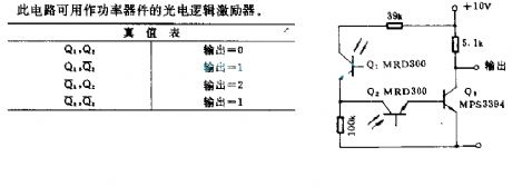
When Q1, Q2 phototransistors taking about 1075.4 IX(100 feet one candle) illumination, the output of Q3 is 0. When one or two phototransistorshave no or little illumination, the output of Q3 is positive or 1.
(View)
View full Circuit Diagram | Comments | Reading(592)
The inside circuit diagram of crystal diode STTH6006TV1、STTH60L6TV、STTH6110TV1
Published:2011/4/1 1:32:00 Author:Ecco | Keyword: crystal diode
The inside circuit diagram of crystal diode STTH6006TV1、STTH60L6TV、STTH6110TV1 is as below:
(View)
View full Circuit Diagram | Comments | Reading(571)
The computer Z RS-23 serial interface current loop circuit diagram
Published:2011/3/30 22:09:00 Author:Ecco | Keyword: serial interface, current loop
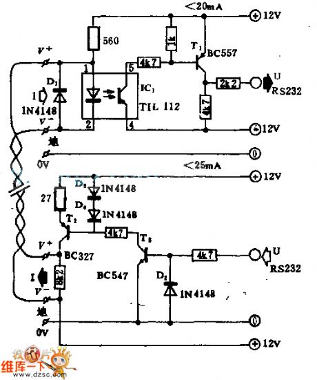
This circuitry is used for the joggle between computer Z RS-23 serial connecting current ring and current ring circuitry, it can transform the voltage semaphore of transmission into the current semaphore with 20 mA, the biggest speed can reach 1200 bits.
Light-coupled device IC3, T1 make up receiving port connecting interface circuit, T2, T3 constitute transmitting terminal interface circuit. When the source is 12V, T2, T3 deliver energy, the current will be sent to IC1 by the circuitry from T2, and pass light-emitted diode of IC1, return to the transmitting terminal again, and the current is about 20mA. When the source is -12V, T2, T3 wil be cut off, and there is no current in circuitry. When transmitting terminal IC1 passes current, the receiving terminal will be breakovering, T1 is ON. And T1 is cut off, the signal of -12V will be sent to RS-232 by R4. From here, the circuitry realizes transmitting figure semaphore by using current ring.
(View)
View full Circuit Diagram | Comments | Reading(2938)
| Pages:2037/2234 At 2020212022202320242025202620272028202920302031203220332034203520362037203820392040Under 20 |
Circuit Categories
power supply circuit
Amplifier Circuit
Basic Circuit
LED and Light Circuit
Sensor Circuit
Signal Processing
Electrical Equipment Circuit
Control Circuit
Remote Control Circuit
A/D-D/A Converter Circuit
Audio Circuit
Measuring and Test Circuit
Communication Circuit
Computer-Related Circuit
555 Circuit
Automotive Circuit
Repairing Circuit