
Circuit Diagram
Index 2020
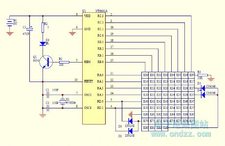
Cable test circuit
Published:2011/4/24 21:49:00 Author:Ecco | Keyword: Cable, test circuit
View full Circuit Diagram | Comments | Reading(1308)
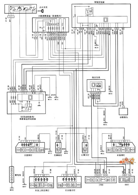
DONGFENG CITROEN Xsars cooling system(manual transmission) circuit diagram
Published:2011/4/24 21:37:00 Author:muriel | Keyword: DONGFENG CITROEN Xsars , cooling system(manual transmission)
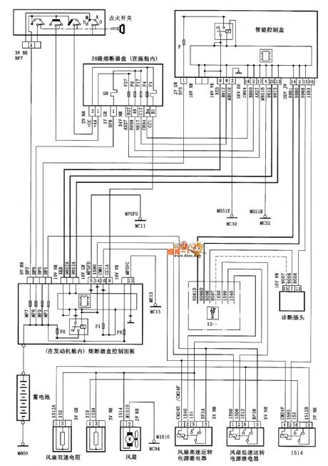
DONGFENG CITROEN Xsars cooling system(manual transmission) circuit diagram is as shown
(View)
View full Circuit Diagram | Comments | Reading(739)
DONGFENG CITROEN Xsars cooling system(automatic transmission) circuit diagram
Published:2011/4/24 21:37:00 Author:muriel | Keyword: DONGFENG CITROEN Xsars, cooling system(automatic transmission)
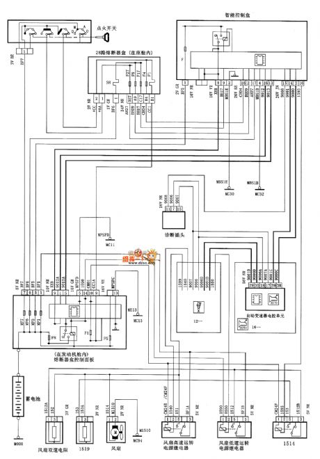
DONGFENG CITROEN Xsars cooling system(automatic transmission) circuit diagram is as shown
(View)
View full Circuit Diagram | Comments | Reading(845)
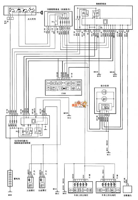
DONGFENG CITROEN XSARA automatic transmission circuit diagram
Published:2011/4/24 20:57:00 Author:muriel | Keyword: DONGFENG CITROEN XSARA, automatic transmission
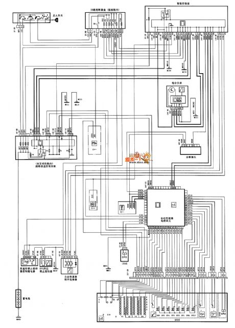
DONGFENG CITROEN XSARA automatic transmission circuit diagram is as shown
(View)
View full Circuit Diagram | Comments | Reading(2989)
DONGFENG CITROEN Xsars fog lamp circuit diagram
Published:2011/4/24 21:38:00 Author:muriel | Keyword: DONGFENG CITROEN Xsars , fog lamp
DONGFENG CITROEN Xsars fog lamp circuit diagram is as shown
(View)
View full Circuit Diagram | Comments | Reading(651)
DONGFENG CITROEN Xsars width lamp circuit diagram
Published:2011/4/24 21:38:00 Author:muriel | Keyword: DONGFENG CITROEN Xsars, width lamp
DONGFENG CITROEN Xsars width lamp circuit diagram is as shown
(View)
View full Circuit Diagram | Comments | Reading(572)
Timing doorbell circuit diagram with CW9300
Published:2011/4/21 21:40:00 Author:muriel | Keyword: Timing doorbell
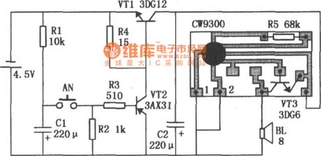
Timing doorbell circuit with CW9300:
As shown is Timing doorbell circuit diagram with CW9300. It has timing function, when we push the button,it will play musicforsome seconds, if we re-push the button immediately after loosing it, the doorbell will not ring either. (View)
View full Circuit Diagram | Comments | Reading(1267)
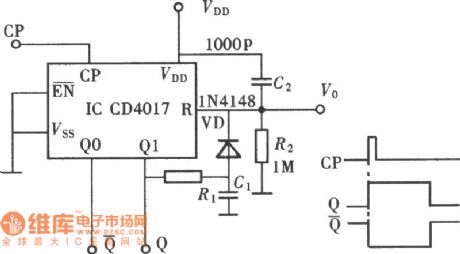
Mono-stable Trigger Circuit Composed of CD4017
Published:2011/4/24 21:17:00 Author:Sue | Keyword: Mono-stable, Trigger
View full Circuit Diagram | Comments | Reading(710)
Accurate Timing Circuit Used to Adjust Capacitor Tolerance
Published:2011/4/24 21:05:00 Author:Sue | Keyword: Accurate, Timing, Capacitor Tolerance
View full Circuit Diagram | Comments | Reading(696)
1kHz Wien Bridge Signal Generator Circuit Composed of LM358
Published:2011/4/24 20:50:00 Author:Sue | Keyword: 1kHz Wien Bridge, Signal, Generator
As seen in the figure is 1kHz signal generator composed of components such as double operational amplifier LM358, Rl~R15, Cl~C5 and so on. The 1kHz weak signal generated from Wien Bridge(C2、C3、R4 and R6) is amplified by A1, and then is buffer amplified by operational amplifier A2 and A3. These two OPRAMs have the opposite output, making a double-end balanced output out of a single-end one. (View)
View full Circuit Diagram | Comments | Reading(1676)
Electronic Tuner Circuit Composed of CC4040
Published:2011/4/22 20:30:00 Author:Sue | Keyword: Electric, Tuner,
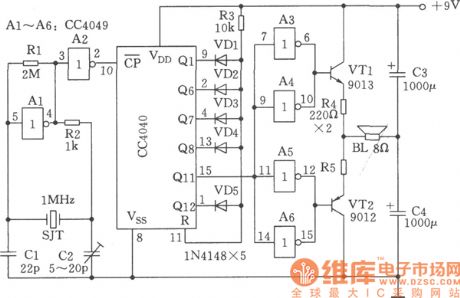
As seen in the figure is the electronic tuner circuit. It can generate International standarded A-tone of 440Hz and can be used as tuner for band. (View)
View full Circuit Diagram | Comments | Reading(867)
Bistable Trigger Circuit Composed of CD4017
Published:2011/4/24 21:20:00 Author:Sue | Keyword: Bistable, Trigger
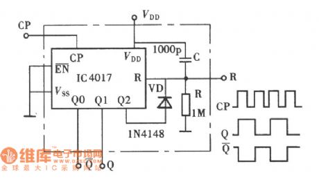
View full Circuit Diagram | Comments | Reading(730)
Frequency Signal Trace Circuit(PLL) Composed of CD4046
Published:2011/4/24 21:02:00 Author:Sue | Keyword: Frequency Signal, Trace, (PLL)
View full Circuit Diagram | Comments | Reading(684)
Multiple Sound Generator Circuit Composed of HT2880
Published:2011/4/21 23:07:00 Author:Sue | Keyword: Multiple, Sound, Generator
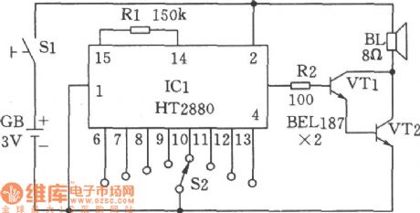
This circuit is able to generate 8 kinds of sounds: 2 kinds of machine guns sound, 2 kinds of bomb sound, dual-tone melody, game sound, animal sound and rifle sound. These sounds can be played by thumb-rotated switch S2 and a push-button switch. HT2880 is ROM chip of a large scale integrated circuit CMOS. In the circuit, transistor VT1 and VT2 are linked into Darlington geminate transistor to amplify signals output from the fourth terminal. (View)
View full Circuit Diagram | Comments | Reading(3675)
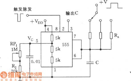
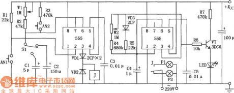
Dark Room Time Controller Circuit Composed of 555
Published:2011/4/24 21:12:00 Author:Sue | Keyword: Dark Room, Time Controller, 555
View full Circuit Diagram | Comments | Reading(634)
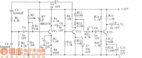
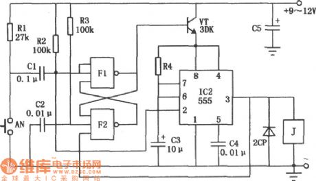
Homemade Simulated Gunshot Generator Circuit
Published:2011/4/22 20:27:00 Author:Sue | Keyword: Homemade, Simulated, Gunshot, Generator
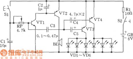
Complementary audio oscillator composed of two transistors can be used as simulated gunshot generator, and the homemade gunshot is very realistic with lingering sound. As seen in the figure, the selections of components are as follows: Triode VT1,VT2: 9014, β=85-115; VT3,VT4: 9015, β=65-85. S1: AN4; S2: KN3. Light emitting diode VD1~VD6: BT201(other types can be used, but luminotrons with low forward voltage and high luminous efficiency are better). Cell GB: 4F22DC6V laminated cells. Loudspeaker BL: 8Ω 0.25W. (View)
View full Circuit Diagram | Comments | Reading(1134)
Low Power Consumption Timer Circuit Composed of 555
Published:2011/4/24 21:15:00 Author:Sue | Keyword: Low Power Consumption, Timer, 555
View full Circuit Diagram | Comments | Reading(938)
Long Period Connected/Disconnected Multivibrator Circuit
Published:2011/4/21 21:03:00 Author:Sue | Keyword: Long Period, Connected/Disconnected, Multivibrator
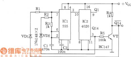
Multivibrator composed of 555 Timer IC can adjust the frequency and duty cycle separately, but when connected/disconnected period is long, a large capacitor is needed. As seen in the figure, however, without a large capacitor, adjustable connected/disconnected period can be realised, with the longest period reaching several hours. A 14-grade binary counter CD4020 is used to count the divided frequency, while the output terminals of CD4020, Q14 and Q14, are connected to R1 and R2 on the rising and falling edge, to output independent connected and disconnected period. The output terminal Q1 can be used to indicate the output of lasting periods. when R2=100k, Ton≈5minutes; when R1=1M, Toff≈50minutes. (View)
View full Circuit Diagram | Comments | Reading(720)
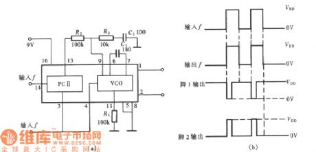
Mono-stable Multivibrator Circuit Composed of 74HCT221 with Variable Duty Cycle
Published:2011/4/21 20:54:00 Author:Sue | Keyword: Mono-stable, Multivibrator, Variable Duty Cycle
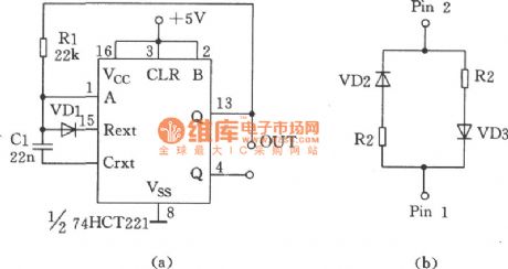
As seen in the figure is the mono-stable multivibrator composed of 74HCT221 with variable duty cycle. Capacitor C is charged and discharged at the same rate, with a duty cycle of 50% and its oscillatory period T equals to RC. In figure (a), R can be replaced by what in figure (b) to get othernecessary duty cycles. In this condition, C1 is charged through R1 and discharged through R2. The oscillatory period T is (R1+R2)C/2 and duty cycle equals to R1/(R1+R2) thereabout. In figure 9-11, VD1,VD2,VD3 refer to type 1N4148. (View)
View full Circuit Diagram | Comments | Reading(688)
Three phase three-wire system phase failure protection circuit
Published:2011/4/24 21:20:00 Author:Nicole | Keyword: three phase, three-wire system, phase failure
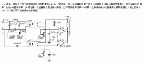
This is a three phase three-wire system power supply phase failure protection circuit, if lacking any phase of A, B, C, the optic coupler output level is lower than the reference voltage of comparator reverse-phase input terminal, comparator outputs low level, to lock PWM drive singal, cuting off the power supply. If changing the comparator input polarity, it also can use high level to lock PWM singal. This phase failure protection circuit adopts optical coupler to isolate heavy current, it is secure and reliable, RP1, RP2 is used to adjust phase failure protection motion threshold value. (View)
View full Circuit Diagram | Comments | Reading(2435)
| Pages:2020/2234 At 2020012002200320042005200620072008200920102011201220132014201520162017201820192020Under 20 |
Circuit Categories
power supply circuit
Amplifier Circuit
Basic Circuit
LED and Light Circuit
Sensor Circuit
Signal Processing
Electrical Equipment Circuit
Control Circuit
Remote Control Circuit
A/D-D/A Converter Circuit
Audio Circuit
Measuring and Test Circuit
Communication Circuit
Computer-Related Circuit
555 Circuit
Automotive Circuit
Repairing Circuit