
Circuit Diagram
Index 2006
555 simple and practical gust circuit
Published:2011/4/26 1:34:00 Author:Ecco | Keyword: 555 , simple , practical , gust circuit
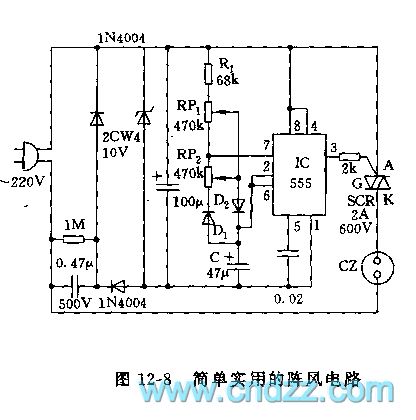
The circuit shown as the figure 12-8 consists of step-down rectifier and vibration control. The supply voltage VDD of IC (555) is about 10V. Because of the connection C, once getting power, 555 sets, SCR trigger is conducted, CZ has power, fan operates. When the threshold level of C is charged to be higher than 2/3, the 555 resets and fan stops. The stopping time of fan, that means t discharge = 0.693RP2C; fan operation time, t charge = 0.693 (R1 + RP1) C.
(View)
View full Circuit Diagram | Comments | Reading(2201)
555 imitating natural wind circuit 2
Published:2011/4/25 22:29:00 Author:Ecco | Keyword: 555 , imitating , natural wind
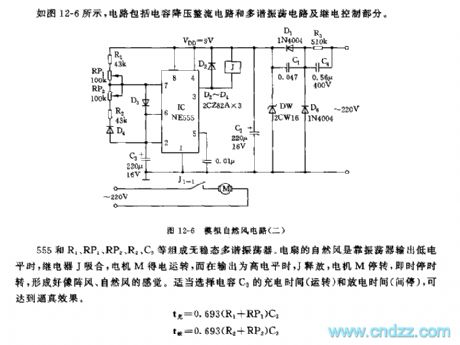
As shown in Figure 12-6, the circuit includes the capacitor step-down rectifier circuit and multivibrator circuit and relay control section. 555 and R1, RP1, RP2, R2, C3 and other components form an astable multivibrator. The natural wind of fan is based on the low oscillator output, the relay J pullling could make the motor M operate, while the output is high, J releases, the motor M stops. That is the motor turns on and off intermittent, and the feeling is like gust, natural wind. Proper selection of charging time and discharging time of capacitor C3 can achieve realistic results.
(View)
View full Circuit Diagram | Comments | Reading(771)
555 simple transistors tester circuit
Published:2011/4/26 1:08:00 Author:Ecco | Keyword: 555 , simple, transistors , tester
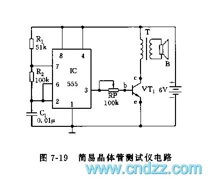
As shown in Figure 7-19, the test instrument is composed of the non-steady-state multivibrator composed of 555 and R1, R2, C1 and the driver of tested grades crystals. It can measure the quality of NPN transistor and estimate B value, the oscillator's oscillation frequency f = 1.44 / (R1 +2 R2) C1. Icon parameter oscillation frequency is about 850Hz. If you plug in the tube, no sound means bad tube; if the sound is small, it indicates that B is low, while loud, B is high.
(View)
View full Circuit Diagram | Comments | Reading(2094)
Various waveforms generator
Published:2011/4/20 21:27:00 Author:Ecco | Keyword: Various , waveform , generator
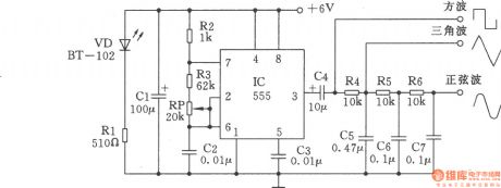
The circuit shown as the chart, it can produce square wave, triangle wave, sine wave and output at the same time, it is especially for the electronic hobbyist or student to do oscilloscope waveform observation experiments. The signal generator circuit is simple, low-cost, easy to adjust. 555 timer connecting as a multivibrator, C2 is the timing capacitor, the charging circuit of C2 is R2 → R3 → RP → C2; C2 discharging circuit is C2 → RP → R3 → pin 7 of IC (discharging tube). The value of R3 + RP is higher than R2, so the charging and discharging time time constants is approximately equal, the pin 3 of IC outputs an approximately symmetrical square wave. Device parameters are as shown, the frequency is about 1kHz, adjusting potentiometer RP can change the oscillator frequency. Square-wave signal becomes triangular wave by the R4, C5 integration network. Triangle wave becomes sine wave by R5, C6 integral network. C1 is the power supply filter capacitor . The light-emitting diode VD is used as power indicator. (View)
View full Circuit Diagram | Comments | Reading(10557)
555 overvoltage, undervoltage delay automatical protection circuit
Published:2011/4/26 1:21:00 Author:Ecco | Keyword: 555 , overvoltage, undervoltage , delay , automatical , protection circuit
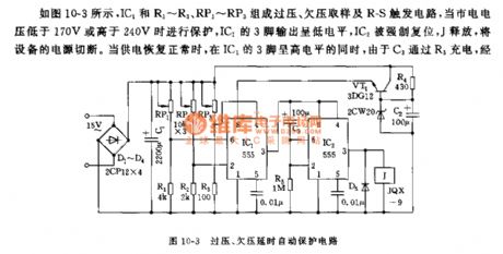
As shown in Figure 10-3, IC1 and R1 ~ R3, RP1 ~ RP3 form overvoltage, undervoltage sampling and R-S trigger circuit, when the mains voltage is below 170V or above 240V, it will be protected in time, IC1's pin 3 output is in low level, IC2 is forced to reset, J releases, power is cut off. When power is restored, pin 3 of IC1 is in high level, C3 is charged through R5, after td = 1.1R5C3, which is about 6 minutes, pin 2is lower than the potential of 1/3 VDD, IC2 sets , J pulls in, the device gets power.
(View)
View full Circuit Diagram | Comments | Reading(1098)
Crystal oscillator and divider(74LS04)
Published:2011/4/20 7:02:00 Author:Ecco | Keyword: Crystal oscillator , divider
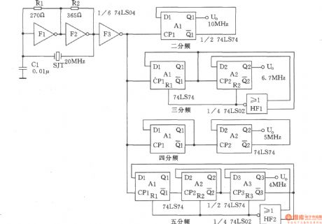
View full Circuit Diagram | Comments | Reading(1775)
RC sine-wave generator composed of LM741CN
Published:2011/4/20 21:40:00 Author:Ecco | Keyword: RC , sine-wave generator
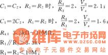
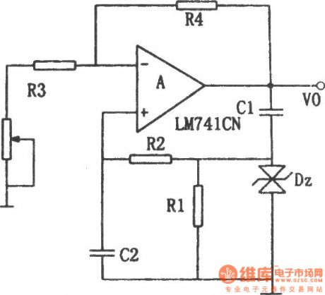
The chart shows the RC sine-wave generator. The components can be selected according to the following formula:
(View)
View full Circuit Diagram | Comments | Reading(2325)
555 refrigerator protection circuit 1
Published:2011/4/25 22:57:00 Author:Ecco | Keyword: 555 , refrigerator , protection
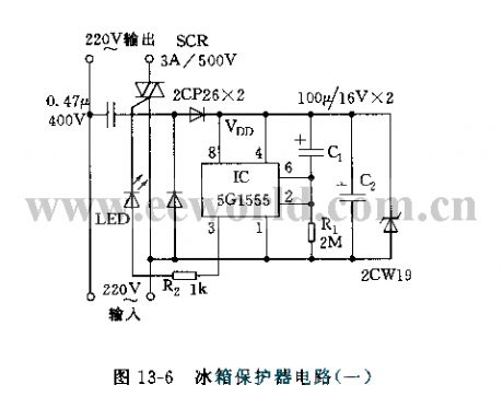
The circuit is shown in Figure 13-6, the circuit is based on 555circuit to form power delay protection circuit. The connection of C1 makes pin 6 be in high level, and pin 3 be in low level when the power failure and supply again, SCR is cut off.
C1 charges, so the pin 2 is lower than the trigger time of 1/3 vdd, that is the delay time td.
Icon corresponding td parameter is about 6 minutes. Setting to 55, pin 3 outputs high level. SCR turns on, the refrigerator gets power and the working indicator LED is lit.
(View)
View full Circuit Diagram | Comments | Reading(973)
36V electric car battery charger circuit diagram
Published:2011/4/26 2:17:00 Author:Rebekka | Keyword: electric car , battery charger
36V electric car battery charger circuit diagram is shown as above. (View)
View full Circuit Diagram | Comments | Reading(10010)
Monitor and TV high-voltage (KV level) protection circuit diagram
Published:2011/4/26 2:13:00 Author:Rebekka | Keyword: Monitor, TV , high-voltage protection
Monitor and TV high-voltage (KV level) protection circuit diagram is shown as above. (View)
View full Circuit Diagram | Comments | Reading(2005)
Beijing grand cherokee car charging marine system circuit diagram
Published:2011/4/26 2:11:00 Author:Rebekka | Keyword: Beijing grand cherokee, car charging marine system
Beijing grand cherokee car charging marine system circuit diagram is shown as above. (View)
View full Circuit Diagram | Comments | Reading(502)
Beijing grand cherokee car start system circuit diagram 3
Published:2011/4/26 2:09:00 Author:Rebekka | Keyword: Beijing grand cherokee car, start system
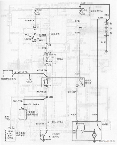
Beijing grand cherokee car start system circuit diagram is shown as above. (View)
View full Circuit Diagram | Comments | Reading(736)
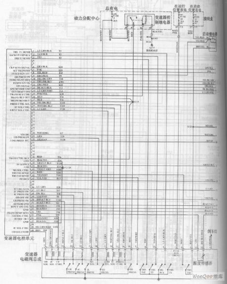
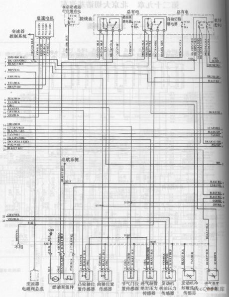
Beijing grand cherokee car automatic transmission circuit diagram 3
Published:2011/4/26 2:08:00 Author:Rebekka | Keyword: Beijing grand cherokee car, automatic transmission

Beijing grand cherokee car automatic transmission circuit diagram is shown as above. (View)
View full Circuit Diagram | Comments | Reading(806)
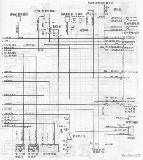
Beijing grand cherokee car engine circuit diagram 3
Published:2011/4/26 2:01:00 Author:Rebekka | Keyword: Beijing grand cherokee, car engine
Beijing grand cherokee car engine circuit diagram is shown as below. (View)
View full Circuit Diagram | Comments | Reading(498)
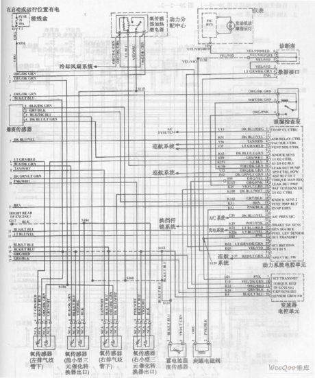
Beijing grand cherokee car dynamic transmission circuit diagram 1
Published:2011/4/26 2:03:00 Author:Rebekka | Keyword: Beijing grand cherokee car , dynamic transmission
Beijing grand cherokee car dynamic transmission circuit diagram is shown as above. (View)
View full Circuit Diagram | Comments | Reading(527)
Beijing grand cherokee car dynamic transmission circuit diagram 2
Published:2011/4/26 2:04:00 Author:Rebekka | Keyword: Beijing grand cherokee , car dynamic transmission
Beijing grand cherokee car dynamic transmission circuit diagram is shown as above. (View)
View full Circuit Diagram | Comments | Reading(473)
555 darkroom timer circuit 3
Published:2011/4/25 22:55:00 Author:Ecco | Keyword: 555, darkroom , timer circuit

As the figure 17-16 shown, the timing circuit is composed of two branches of 555, IC1 forms a timer, IC2 is a second signal metronome. AN1 is the timer button, clicking the AN1, 555 sets, J pulls in, light exposure lamp H1 is lit, safelight H2 is off. K1 is regular file, when the C1 (or C2) is charged to more than 2/3 threshold level, the 555 resets, J releases. H1 is off, H2 is lit, exposure ended. IC2 and RP2, R4, R5, C4 etc. form astable multivibrator, adjusting the RP2 make the oscillation be 1Hz. The output of drives red LED light by VT1.
(View)
View full Circuit Diagram | Comments | Reading(903)
555 Timekeeping audio circuit
Published:2011/4/25 22:18:00 Author:Ecco | Keyword: 555 , Timekeeping , audio circuit
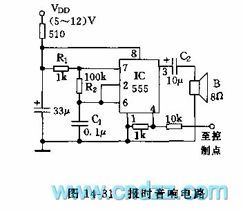
The circuit is shown in Figure 14-31, it is a timing signal controlled multivibrator composed of 555. Pin 4 of 555 is the force reset terminal, when the pin voltage drops below 0.4V, the circuit will go to non-trigger state. Using the foot control to external timing signals, usually it shows a low potential, while the voltage of time signal being higher than 1V, the circuit turns and issues an audio time signal with about 400Hz. Pin 4 of 555 is connected to the output clock timing, or connected to the security and other sensing devices deflection point by a 10kΩ resistor. Once there is a high mutation, the speaker will issue a hasty sound, the parameters of oscillator can be changed by the R1, R2, C1.
(View)
View full Circuit Diagram | Comments | Reading(701)
Mileage/N consumption counting circuit
Published:2011/4/25 21:30:00 Author:Nicole | Keyword: mileage
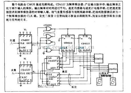
The circuit is composed of CMOS IC. CD4527 is frequency multiplicator, it produces output pulse series, the output frequency is in direct proportion to the product of two inputs. The time is shared by the output frequency. The speed sensor is series with speed indicator cable, it feeds speed data to the clock input terminal of frequency multiplicator. transducer of oil gas flow is series with gasoline consumption line, it feeds gasoline consumption data to CLK terminal of another frequency multiplicator. LED 2 bit digital codes can display the gasoline consumption constantly, the shown nember represents the relation between gasoline consumption and mileage. (View)
View full Circuit Diagram | Comments | Reading(1005)
Beijing grand cherokee car engine circuit diagram 2
Published:2011/4/26 2:00:00 Author:Rebekka | Keyword: Beijing grand cherokee, car engine
Beijing grand cherokee car engine circuit diagram is shown as below. (View)
View full Circuit Diagram | Comments | Reading(583)
| Pages:2006/2234 At 2020012002200320042005200620072008200920102011201220132014201520162017201820192020Under 20 |
Circuit Categories
power supply circuit
Amplifier Circuit
Basic Circuit
LED and Light Circuit
Sensor Circuit
Signal Processing
Electrical Equipment Circuit
Control Circuit
Remote Control Circuit
A/D-D/A Converter Circuit
Audio Circuit
Measuring and Test Circuit
Communication Circuit
Computer-Related Circuit
555 Circuit
Automotive Circuit
Repairing Circuit