
Circuit Diagram
Index 2017
Three phase SCR trigger
Published:2011/4/25 3:05:00 Author:Nicole | Keyword: three phase SCR, trigger

XMA5000 series regulator sends out three phase SCR trigger pulse instruction, and it emits six SCR phase shift trigger or zero-crossing trigger control singal, it is used to control the main loop SCR trigger conduction. It adopts unique trigger control circuit, it can trigger 3A~1000A unidirectional or bidirectional SCR.
(View)
View full Circuit Diagram | Comments | Reading(1896)
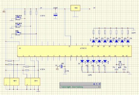
Vehicle flashing lights controller 3
Published:2011/4/21 4:09:00 Author:Ecco | Keyword: Vehicle , flashing lights , controller
(View)
View full Circuit Diagram | Comments | Reading(658)
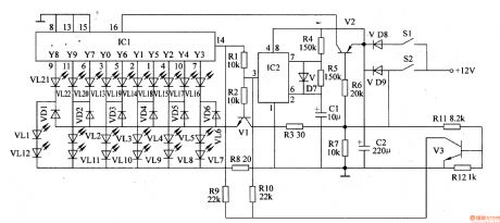
Vehicle flashing lights controller 2
Published:2011/4/21 3:54:00 Author:Ecco | Keyword: Vehicle , flashing lights , controller
The motor vehicle flashing lights controller described in the example is composed of LED light-emitting diodes and the relative control circuit. The LED light-emitting diodes are made in various designs and installed of the rear window part of the motorcycle or car, when driving at night, the light-emitting diode is lit like the water cycle; when braking, all light-emitting diode are flashing to remind the following vehicle.
The working principleThe motor vehicle flashing lights controller is composed of electronic filter circuit, the multivibrator circuit and the LED control display circuit, it is shown in Figure 7-26.
When the YO or Y6 of IC outputs high level, VLl light emitting diode in 1 Road is lit.
When the Y1 or Y5 of IC outputs high level, VL2 light emitting diode in2 Road is lit.
When the Y3 of IC outputs high level, VL4 light emitting diode in4 Road is lit.
When the Y7 or Y9 of IC outputs high level, VL3 light emitting diode in5 Road is lit.
When the Y2 or Y4 of IC outputs high level, VLl light emitting diode in3 Road is lit.
When the Y8 of IC outputs high level, VL6 light emitting diode in6 Road is lit.
(View)
View full Circuit Diagram | Comments | Reading(1334)
8515 extending RAM circuit diagram
Published:2011/4/25 2:46:00 Author:Ecco | Keyword: extending, RAM
View full Circuit Diagram | Comments | Reading(580)
Motor vehicle steering flasher 1
Published:2011/4/21 1:57:00 Author:Ecco | Keyword: Motor vehicle, steering flasher
(View)
View full Circuit Diagram | Comments | Reading(512)
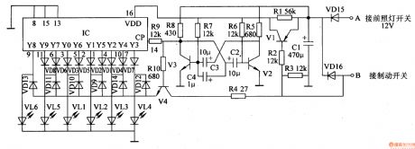
Motor vehicle steering flasher 11
Published:2011/4/21 22:07:00 Author:Ecco | Keyword: Motor vehicle, steering flasher

The motor vehicle steering flasher described in the example is a non-contact electronic flash which uses a VMOS power field effect transistor and 555 time base circuit. It has the features of long life, good effects, alternative use of magnetic motor steering and electronic flasher.
The working principle
The motor vehicle steering flasher circuit is composed of multivibrator, audio driver and flash control circuit, it is shown in Figure 7-20.
Multivibrator circuit consists of time-base integrated circuit IC, resistor Rl, saturated capacitors Cl, C2.
Audio driver circuitis composed ofthe resistor R3, transistor V, and the speaker BL.
Flash control circuit is composed of VF power field effect transistors by the VMOS, diode VDl, VD2, resistors R4, turn signal HLl-HL4 and turn signal switch S.
Component selection
RI-R4 selects 1/4W carbon film resistor or metal film resistors.
Cl selects electrolytic capacitor with voltage in 16V; C2 uses polyester capacitorsor monolithic capacitor. (View)
View full Circuit Diagram | Comments | Reading(555)
How to use 74LS138 cascaded forming 000~1FF addressing space?
Published:2011/4/25 2:39:00 Author:Ecco | Keyword: cascaded , 000~1FF , addressing space
View full Circuit Diagram | Comments | Reading(828)
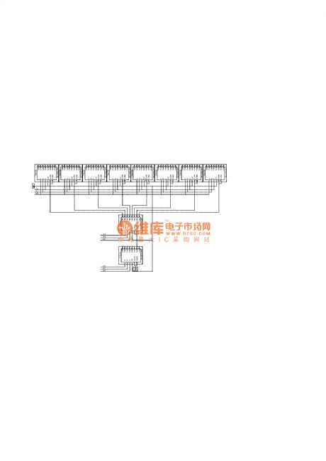
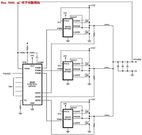
The motherboard two-phase three-phase power supply circuit diagram 02
Published:2011/4/25 2:34:00 Author:Ecco | Keyword: motherboard , two-phase , three-phase , power supply
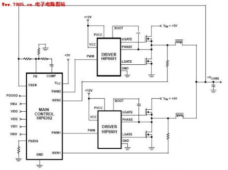
View full Circuit Diagram | Comments | Reading(2567)
The motherboard two-phase three-phase power supply circuit diagram
Published:2011/4/25 2:32:00 Author:Ecco | Keyword: motherboard , two-phase , three-phase , power supply
View full Circuit Diagram | Comments | Reading(1819)
Distribution diagram of each pin of p4 478 chip
Published:2011/4/25 2:20:00 Author:Ecco | Keyword: Distribution , each pin , chip
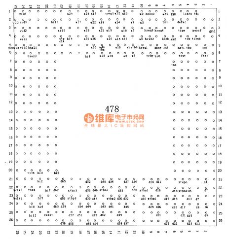
View full Circuit Diagram | Comments | Reading(557)
The hardware circuit of monolithic electronic hard disk controlled by SST89C58
Published:2011/4/25 2:23:00 Author:Ecco | Keyword: hardware circuit , monolithic, electronic , hard disk
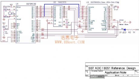
View full Circuit Diagram | Comments | Reading(861)
Serial turning Infrared circuit
Published:2011/4/25 2:27:00 Author:Ecco | Keyword: Serial , turning , Infrared
View full Circuit Diagram | Comments | Reading(546)
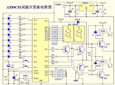
Microcontroller test board circuit 2
Published:2011/4/25 1:51:00 Author:Ecco | Keyword: Microcontroller , test board
View full Circuit Diagram | Comments | Reading(947)
at89c51 DIY Programmer(English)
Published:2011/4/25 2:10:00 Author:Ecco | Keyword: DIY , Programmer
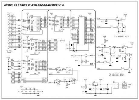
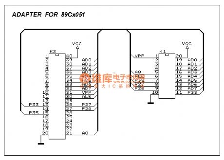
Figure 1 shows the circuit diagram of the Flash Programmer, the programmer is interfaced with the standard parallel port of the PC. As shown in the diagram U2 is used to control the data flow between the controller and the PC, U4 latched the low order address byte and U5 latched the high order address byte, while U3 is used to generate the control signals for micro controller to be programmed. IC U1 is used to generate the progrram pulse for the u-controller. The power supply section uses U8 to generate the logic 5V supply while the U7 is used to provide the programming supply voltage to controller. IC U6 is used to generate the VDD power supply voltage for the u-controller which is selectable either 5v or 6v5.
The power to the circuit is provided by a wall adapter of 15 to 18V output, normally a 15V type adapter will provide a 19~20V output voltage. As shown in the diagram the crystal X1 can be replaced by a resonator in that case capacitors C4 and C5 are not required. Place a small heatsink on U8 voltage regulator.
For the adjustment of P1, P2 and P3 use a digital multimeter & follow the steps shown below,
1. To adjust P1, temporarily connect T1 base to ground using test clips then adjust P1 to get 6.5V at the output of regulator U6.2. Next first adjust P2 to get the 13.1V at the output of regulator U7, make sure transistor T5 is off or temporarily connect the T5 base to ground using test clips.3. Now temporarily short the collector of transistor T5 to ground using test clips.3. Adjust P3 to get the 12.1V at the output of U7 regulator IC.
Figure 2 shows the circuit diagram of the interface adapter card required for the programming of 20 pin Flash devices.
Pgm89v3.zip file is used to run the programmer. This is a Windows program which can be used underWindows 95 & 98. The main screen of the program is shown in figure 4.
In order to insure safe insertion & removal of the u-controller from programmer ZIF socket make sure programmer power supply is turned on before starting the program and the red LED D1 must be turned off when the program is started. The u-controller should be placed or removed from the ZIF socket when the red LED D1 is off.Also note that the software does not provide the erase command because this function is performed automatically during device programming. If you are required to erase the controller first use the clear buffer command in edit menu then program the controller, this will erase the controller memory. (View)
View full Circuit Diagram | Comments | Reading(4917)
at89c2051 DIY Programmer(English)
Published:2011/4/25 2:17:00 Author:Ecco | Keyword: DIY , Programmer
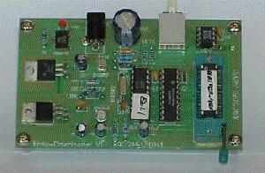
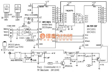
Figure 1 depicts a circuit diagram of the Easy-Downloader. As shown, the circuit uses a 89C2051 with writer.hex firmware, 74LS373 8-bit latch, DS275-like, 7805, LM317 and two transistors, 2N2222A and 2N2907A. The programming voltage control circuit is the same as recommended by ATMEL application note. It can be raised from 0V, 5V and 12V by appropriated signal from P3. The 8-bit latch, 74LS373 provides some signal for selecting the programming modes. A byte to be programmed or read back is sent/received through P1. Incrementing address is done by pulsing a positive pulse to XTAL pin. The circuit may be built using simple point-to-point soldering with a general purpose PCB( fish's egg like PCB) or making PCB shown above, the file is Easy-v1.pcb Protel PCB version 2.76. The finished board should be tested without any chips; 1) +5V supply, 2) programming voltage 0V, 5V and 12V by connecting the pin that control (P3.5 and D) 2N2222A and 2N2907 to +5V and/or GND. The adapter output should be approx. 15Vdc 100mA.
(View)
View full Circuit Diagram | Comments | Reading(3442)
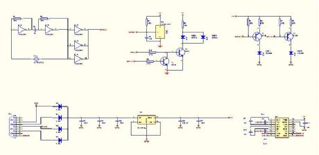
High and low frequency signal generator
Published:2011/4/21 6:31:00 Author:Ecco | Keyword: High frequency, signal generator, low frequency
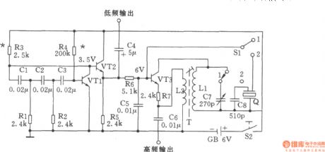
The high and low frequency signal generator shown as the chart can produce low frequency signal with 1kHz, IF signal with 465kHz and high frequency signal with 525 ~ 1605kHz, it can help debug on the radio or other circuit, and it is suitable for beginners. Transistor VTl ~ VT3: selecting 3DGl00, 3DG201 other high-frequency low-power silicon tube, fT> 100MHz, β value is between 50 to 100. C7 uses 7/270pF radio with double or a single connecting capacitor. Oscillation transformer T is restructured on the radio, the core uses a 0.08mm high strength wire with 100 turns and rolled on L1, 35 turns on L2. C8 uses 510pF mica capacitor. Q uses three-stage type of 465kHz IF ceramic filter. Sl uses DPDT switch type. Other values are shown in Figure
(View)
View full Circuit Diagram | Comments | Reading(1479)
Simple high-frequency signal generator
Published:2011/4/20 6:51:00 Author:Ecco | Keyword: Simple , high-frequency , signal generator
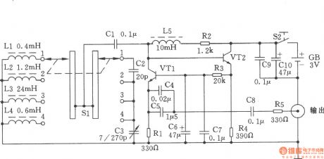
The chart shows a simple high-frequency signal generator. Changing the inductance of LC resonant circuit by the band switch Sl will change the frequency range of high frequency oscillation. This machine can be divided into four stages: the first stage is in 0.4 ~ 2MHz; the second stage is in 2 ~ 10MHz; the third stage is in 9 ~ 45MNz; fourth stage is in 60 ~ 110MHz. Components Selection: VTl, VT2 use the NPN silicon tube with fT ≥ 800MHz, β ≥ 100 of, such as 9018, C535 and so on. All resistors use 1/8W carbon film resistors. Capacitor C5 uses a monolithic capacitor or other ceramic capacitor. L2, L3, L4, L5 use high-frequency magnetic inductors and they can also be self-wound. Ll uses Φ0.6mm high strength wire with 8 flat close turns, and it is wound as the coil with inner diameter in Φ7mm . Sl uses the two-pole four roll band switch.
(View)
View full Circuit Diagram | Comments | Reading(2446)
Three waveform signal generator
Published:2011/4/22 1:40:00 Author:Ecco | Keyword: Three waveform, signal generator
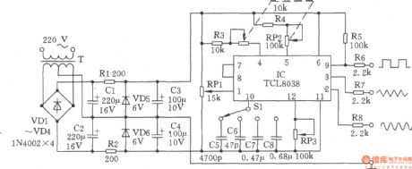
TCL8038 is a dedicated function generator circuit with a variety of waveform output function (square wave, triangle wave, sine wave). The operating current is about l0mA with positive and negative power. the circuit is shown as the chart. C5 ~ C8 use the capacitors with small temperature coefficient and the capacitance error. Sl can output 1Hz pulse when the block being C8. RP2 uses 51 ~ 100kΩ double connection potentiometer to facilitate the frequency scale. RPl, RP3 are used to fine-tune the output waveform and make the upper and lower peaks along the smooth. Sl is the frequency of coarse block, RP2 is fine-tune frequency potentiometer. When debugging, the frequency scale calibration could be made with the aid of a digital frequency meter. And the waveform is measured by oscilloscope, adjusted by the potentiometer RPl and RP3. RPl makes the duty cycle of square wave modulation be 50% , adjusting RP3 could make the sine wave signal tend to be more smooth. The frequency of the signal generator is decided by the formula 0.3/RAv · (C5 ~ C8) and its frequency range is 1Hz ~ 1MHz. (View)
View full Circuit Diagram | Comments | Reading(1111)
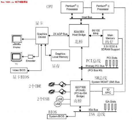
440bx mainboard structure chart
Published:2011/4/25 1:49:00 Author:Ecco | Keyword: mainboard, structure
View full Circuit Diagram | Comments | Reading(1117)
24cxx reproducer circuit
Published:2011/4/25 1:47:00 Author:Ecco | Keyword: reproducer
View full Circuit Diagram | Comments | Reading(969)
| Pages:2017/2234 At 2020012002200320042005200620072008200920102011201220132014201520162017201820192020Under 20 |
Circuit Categories
power supply circuit
Amplifier Circuit
Basic Circuit
LED and Light Circuit
Sensor Circuit
Signal Processing
Electrical Equipment Circuit
Control Circuit
Remote Control Circuit
A/D-D/A Converter Circuit
Audio Circuit
Measuring and Test Circuit
Communication Circuit
Computer-Related Circuit
555 Circuit
Automotive Circuit
Repairing Circuit