
LED and Light Circuit
Index 42
PORTABLE_SCOPE_CALIBRATOR
Published:2009/7/20 3:33:00 Author:Jessie
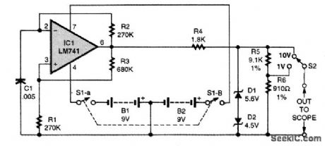
This simple circuit can be used to calibrate scopes or other equipment. (View)
View full Circuit Diagram | Comments | Reading(720)
DELAYED_SWEEP_ADAPTER
Published:2009/7/20 3:26:00 Author:Jessie

The schematic for the delayed sweep adapter is shown in the figure. Power for the circuit is pro-vided by a dual-polarity, 5-V supply. An LM360 high-speed comparator (IC1) with complementary TTL outputs is at the heart of the circuit. A trigger-level control, potentiometer R2, allows the adapter to trigger on any part of the waveform being displayed. With the values shown, the circuit functions well with a Hitachi V-212 oscilloscope, whose channel 1 output is about 25 mV per vertical division of the signal display. Assuming a normal display of about six divisions, the level control pro-vides a range of ±150 mV. You can change that range to suit your scope output by adjusting the ratio of R3 (15,000 Ω) to R4 (470 Ω); however, maintain the ratio of R5 (100,000 Ω) to R4 (470 Ω) for proper hysteresis. Resistor R1 (51 Ω) terminates the 50-Ω cable from the channel 1 output jack. IC2, a 7473 TTL dual J/K flip-flop, is configured in its toggle mode to divide the input frequency by 2. That ensures that IC3, a 74121 TTL monostable multivibrator, will function accurately over the in-put waveform's full time period. The pulse output from IC3 is coupled to the trigger-input jack of your oscilloscope, and the slope is selected via S2 to match the slope selected on your oscilloscope. Po-tentiometer R9 allows fine positioning of the trace and potentiometer R7 allows the output pulse width selected to be multiplied by a factor from x1 to over x2.5. Switch S1 lets you select the de-sired pulse width by switching in C8 through C13, in a 1-2-5 sequence. The adapter circuit was de-signed to operate on an external ±5-V, 100-mA power supply to avoid 60-Hz pickup in the unit. (View)
View full Circuit Diagram | Comments | Reading(2248)
OPTICALLY_ISOLATED_PRECISION_RECTIFIER
Published:2009/7/20 3:24:00 Author:Jessie
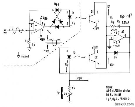


An isolation amplifier and precision rectifier can be combined in one topology, as demonstrated here. It achieves excellent rectification symmetry, zero stability, and good linearity (better than 1 per-cent) and frequency response (>>10kHz), with a minimum of precision components. A1 acts as a volt-age-to-current converter by serving the current through the D1 to D4 bridge and L1. Therefore, the voltage developed across R1 equals the instantaneous input voltage. The diode bridge's full-wave rectification causes L1 to be forward-biased, regardless of the polarity of the input voltage. The magnitude of the bias controls the intensity of optical coupling between L1 and Q1, and, thereby, the magnitude of Q1's collector current. A2 servos the current through L2 and R2 so that the current passed by Q2 balances that passed by Q1. Because of the good tracking of elements of the PS2501-2 dual optoisolator, a constant ratio exists between the L1 and L2 currents. Consequently, R2 can be adjusted so that the out-put voltage across R2 is equal to the rectifier's isolated input voltage. R3 and C1 provide frequency com, pensation for the L2-Q2 feedback loop. D5 prevents potentially destructive reverse bias of L2. (View)
View full Circuit Diagram | Comments | Reading(1387)
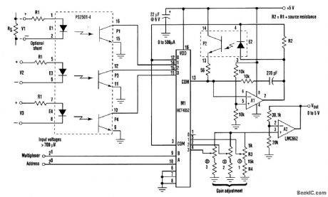
OPTICALLY_ISOLATED_ANALOG_MULTIPLEXER_
Published:2009/7/20 3:21:00 Author:Jessie

The circuit described here provides three channels of optically isolated input that will work for many precision signal-acquisition applications. The only power required is a single 15-V rail with ground common to the analog-to-digital converter. Multiplexer operation is based on an ordinary quad-channel optoisolator (PS2501-4). Each LED (such as E1) in combination with input-scaling resistor R1 will, in response to Vin, pass a current of I1=( Vin- VLED)/(R1+Rs), where VLED-the forward voltage drop of the LED and Rs=the signal source's internal resistance. R1 is chosen to establish a full-scale LED current near 500 μA. Assuming (for example) that channel 1 is selected, the resulting photocurrent in P1 will tend to pull the summing point of A1 low. In response, A1 will forward-bias E2 to generate a balancing photocurrent in P2. The E2 current required to maintain this balance will closely track I1, and the VLED of E2 will be close to the VLED of E1. The current sourced through M1 to the gain-adjustment network is directly proportional to the floating input voltages. Therefore, it is independent of the LED voltage drops. (View)
View full Circuit Diagram | Comments | Reading(2951)
SCOPE_MIXER
Published:2009/7/20 4:12:00 Author:Jessie
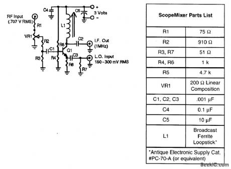
This circuit permits use of a low-frequency scope to view RF signals. The signal to be viewed is mixed with a LO signal about 1 MHz away and the IF output is viewed on the scope. (View)
View full Circuit Diagram | Comments | Reading(814)
DUAL_SCOPE_ADAPTER
Published:2009/7/20 4:11:00 Author:Jessie
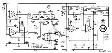
The input stage is the trigger amplifier based on the two channels of an LM319 dual comparator (IC1-a and IC1-b). The in-put signal is taken from the channel 1 output jack of your oscilloscope, and it is applied to J1 on the adapter. The input slope is selected by switch S1, and the signal is coupled to C3 and IC2, the multivibrator stage. Capacitor C3 provides the proper negative-going pulse to trigger IC2, a TLC555 CMOS timing IC. Switch S2 selects the desired range either milliseconds or mi-croseconds-and switch S3 selects the polarity of the output slope. Transistors Q1 and Q2 form a fast (less than 10-ns delay) inverting output stage. The output from switch S3 is ±5 V, which is sufficient for excellent contrast in intensity modulation. It is also satisfactory for stable triggering in the adapter's delayed-sweep mode. Precise input current to capacitors C4 and C5 is supplied from the collector of dual transistor Q3, a 2N5117. It is a dual-matched PNP pair in one package. Operational amplifier IC3, an LF356, is configured as a noninverting follower with gain. Transistor Q3 is configured as an unusual current mirror that unloads the relatively slow operational amplifier, allowing the second half of Q3 to demonstrate its fast dynamic response. A reference voltage is developed across both sets of emitter resistors (R20 to R25) to pro-duce the constant charging current for capacitors C4 and 05. The two sections of switch 54 (S4-a and S4-b) select the range-either 1.0, 10, or 100-in conjunction with switch S2 (milliseconds or microseconds). Zener diodes D6 and D7 permit the operational amplifier outputs to operate in their linear regions. Variable resistor R18 (1 kΩ, 10 turns) is the range multiplier. (View)
View full Circuit Diagram | Comments | Reading(1937)
VOLTAGE_CURSOR_ADAPTER
Published:2009/7/20 4:08:00 Author:Jessie
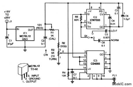
This is the schematic diagram for the voltage cursor adapter. The required 15- to 25-V power to the circuit can be supplied either by batteries or by a wall-mounted ac to 15-Vdc adapter. The MC78L12 voltage regulator (IC1) supplies regulated 12 Vdc to the rest of the circuit. The ICM7555 timer (IC2) drives the CD4066B, a CMOS bilateral switch (IC3). This drive frequency can either be a normal frequency (NORM) of 100 kHz or a low frequency (LO-F) of 10 kHz, depending on the setting of switch S1. Set S1 to LO-F for inputs below 500 Hz. The dc reference voltage supplied to pin 3 of IC3 is set by R3, a 10-turn, 5000-Ω precision potentiometer. The voltage can be read directly from a turns counter dial coupled directly to the potentiometer's wiper. The accuracy of this reading can be 1 per-cent or better. Trimmer potentiometer R1 permits the voltage to R3 to be calibrated to precisely 10 V. The circuit is calibrated by setting the digital reading on the turns counter of R3 to the full clockwise position and adjusting R1 for a reading of 10 V at the wiper of R3 with a digital voltmeter. Bilateral switch IC3 converts the dc reference to a square wave with exactly the same wiper amplitude. The square-wave output appears on the common pins 4, 9, and 10 of IC3 aqd coaxial plug PL1. (View)
View full Circuit Diagram | Comments | Reading(1248)
VOLTAGE_LEVEL_INDICATOR
Published:2009/7/9 21:16:00 Author:May
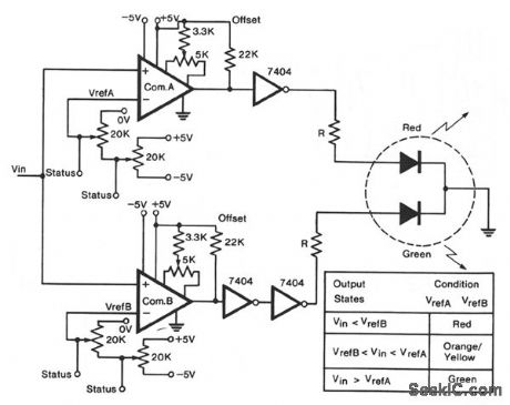
A tricolor LED, acts as the visual indicator of the voltage level. The voltage to be measured is connected to the two comparators in parallel. The first 20-KΩ trimmer defines a voltage between ±5 V and this becomes the full-scale value of the reference voltage. The second trimmer is a fine adjustment to give any reference voltage between 0 V and the full-scale voltage. Thus, it is possible to select both positive and negative reference voltages. During the initialization procedure, a voltage, equal to the reference voltage of each comparator, is connected to the input terminal, and the offset balance potentiometer is adjusted to give a reading between the high and low output voltage levels. The inverter following comp A ensures that, whatever the input voltage, at least one diode is lit. The two inverters following comp B leave the voltage largely unchanged, but provide the current necessary to illuminate the diode. The value of the resistance should be chosen so that the current through any single diode does not exceed the specified limit, usually 30 mA. The LED contains a red and a green diode with a common cathode. When both diodes are lit, a third color, orange, is emitted. With VREFA greater than VrefB, the output states given in the diagram apply. (View)
View full Circuit Diagram | Comments | Reading(0)
VOLTAGE_LEVEL_INDICATOR
Published:2009/7/9 21:16:00 Author:May
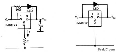
Three-terminal regulator device (LM78LXX) has Vout=Vin, until the input rises 1.5 to 2 V above the output when the regulated voltage Vreg = XX is obtained. A differential of 1.5 V between input and output is necessary to light the LED. Thus, the LED lights when Vin rises above Vreg + IR + 1.5 V, where I is typically 6 mA (a zener diode could be used in place of R). For input voltages much higher than necessary to light the LED, a current-limiting resistor in series might be necessary. A useful automotive application is shown in Fig. 14-9(b). The circuit indicates when battery voltage is above 13.5 V which indicates (in conjunction with gn ammeter) whether the alternator/regulator/battery system is operating correctly. With the engine off, the battery voltage drops to 12 V and the LED extinguishes. The circuit requires no calibration. (View)
View full Circuit Diagram | Comments | Reading(1666)
LOW_BATTERY_INDICATOR
Published:2009/7/9 21:13:00 Author:May
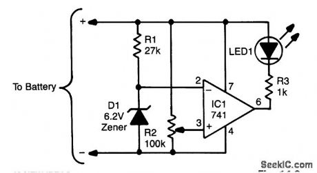
The sensing circuit consists of a 741 op amp set up as a voltage comparator, using a zener diode as a voltage reference. The op amp is inserted as a bridge between two resistance ladders, one which contains the zener reference, and the other a high-value linear potentiometer. When the voltage at the wiper of the potentiometer drops below the voltage set by the zener, the output of the op amp becomes low; that turns on the LED connected between it and VCC. The circuit can be adapted to work with battery-powered circuits that require between 6 and 18 V; the only changes needed would be a lower-voltage zener and a smaller current-limiting resistor in the case of voltage below 9 V, and a larger resistor for higher voltages. (View)
View full Circuit Diagram | Comments | Reading(0)
DUAL_TRACE_CONVERTER
Published:2009/7/20 4:15:00 Author:Jessie
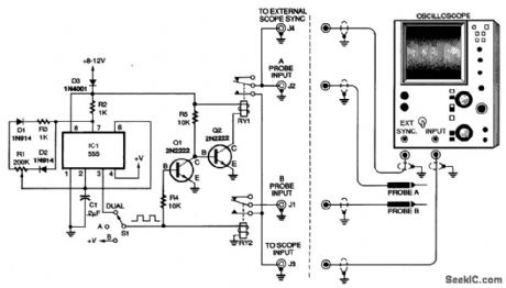
The probe switching circuit is shown in the figure. Two SPST reed relays, RY1 and RY2, switch the signal from two probes to a single scope input. Reed relays provide smooth and noise-free switching. The input side of each relay is connected to a scope probe, and the outputs of the relays are tied together and connected to the scope's single-channel input. A 555 timer, IC1, is con-figured as a variable-duty-cycle square-wave oscillator. Potentiometer R1 varies the oscillator's duty cycle to compensate for response-time variations that different relays might have. The potentiometer is adjusted to give equal brightness to both of the signals being displayed on the oscilloscope. If the relays you choose work well with a 50-percent duty cycle, the potentiometer can be replaced with two fixed resistors wired in series, with the junction between the two resistors connected to pin 2 of IC1. With the parts values shown, the timer has an output frequency of about 80 Hz. Switch S1 allows independent viewing of each oscilloscope trace. When S1 connects pin 3 of IC1 to the coil of RY2 and R4, both input traces will be displayed. When S1 connects +V to the coil of RY2 and R4, only channel B will be displayed. With the switch in the center OFF position, only the channel-A signal is displayed. (View)
View full Circuit Diagram | Comments | Reading(1141)
WIDE_RANGE_DIGITALLY_CONTROLLED_VARIABLE_GAIN_AMPLIFIER
Published:2009/7/9 21:02:00 Author:May
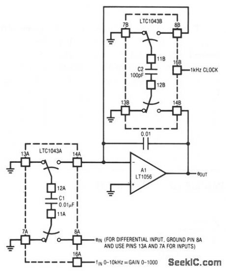
The circuit uses the LTC1043 in a variable gam amplifier which features continuously variable gain, gain stability of 20 ppm/℃, and single-ended or differential inputs. The circuit uses two separate LTC1043s. LTC1043B is continuously clocked by a 1-kHz source, which could also be processor supplied. Both LTC1043s function as the sampled data equivalent of a resistor within the bandwidth set by A1's 0.01-μF value and the switched-capacitor equivalent feedback resistor. The time-averaged current delivered to the summing point by LTC-1043A is a function of the 0.01-μF capacitor's input-derived voltage and the commutation frequency at pin 16. Low-commutation frequencies result in small time-averaged current values, and require a large input resistor. Higher frequencies require an equivalent small input resistor. (View)
View full Circuit Diagram | Comments | Reading(765)
SCOPE_CALIBRATOR
Published:2009/7/20 4:05:00 Author:Jessie
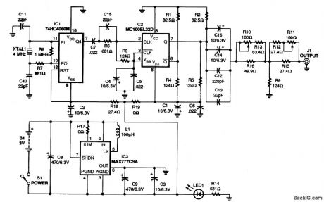
A 74HC4060 HCMOS oscillator/divider integrated circuit (IC1)was chosen for generating the master clock Choosing that part lets us use an inexpensive 4-MHz crystal The divide-by-16 output of IC1, at 250 kHz, is applied to a Motorola MC100EL32 divide-by-2 ECLips flip-flop (IC2) through level shift and decoupling components C7.015, and R6 Resistor R3 sets the input impedance seel1 by IC2 and divides the amplitude of IC1's output down to the ECLips input levels The MC100EL32 has transition times of both outputs specified at less than 350 ps (0.35 ns)and temperature-compensated output levels The divide-by-2 action of the device provides 125 kHz at approximately 800 mV p-p to the amplitude adjustment circuit and output stage. The output of IC2 is terminated with loads consisting of resistor pairs R1-R4 and R2-R5. The values shown provide an equivalent load voltage of about -2 V and a load impedance of 50 Ω. The output of IC2 is ac-coupled by capacitors C12, C13, C14, and C16 to an adjustable T-attenuator network. The various values of the coupling capacitors combine to transmit the fat rise-time edges (C12 and C13) while preventing droop at the 125-kHz base frequency (C14 and C16). (View)
View full Circuit Diagram | Comments | Reading(0)
INERARED_
Published:2009/7/9 20:37:00 Author:May
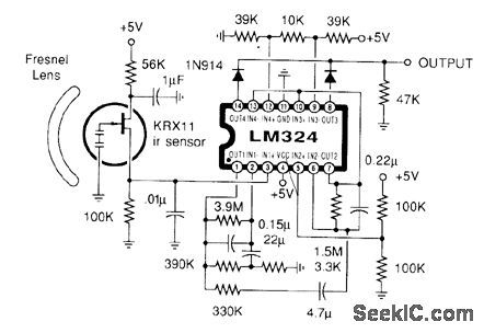
This circuit uses an Amperex pyroelectric IR sensor, an LM324 op amp (conftgured as a high-gain amplifier in the 0.3-to 5-Hz range), and a win-dow detector. The output will go high on any motion, which will change the infrared signature seen by the sensor. (View)
View full Circuit Diagram | Comments | Reading(10308)
IR_DETECTOR
Published:2009/7/9 20:29:00 Author:May
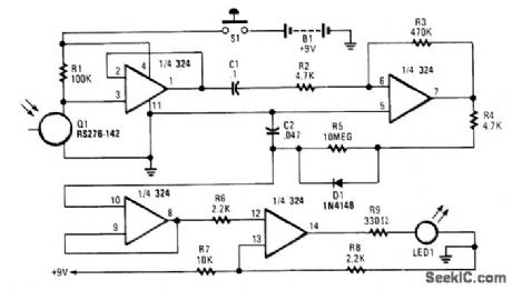

Useful for checking TV remote controls, IR-based alarm systems, and IR sources, this circuit causes LED1 to turn on for two seconds in the presence of IR light pulses. U1A acts as a voltage follower for detector Q1. C1 and R2 form a differentiating network and U1B acts as an amplifier for the pulses, which charges C2. Voltage follower U1C samples the voltage on C2 and drives comparator U1D, which switches LED1 on or off.
(View)
View full Circuit Diagram | Comments | Reading(1710)
TRANSMITTER_OUTPUT_INDICATOR
Published:2009/7/9 5:38:00 Author:May
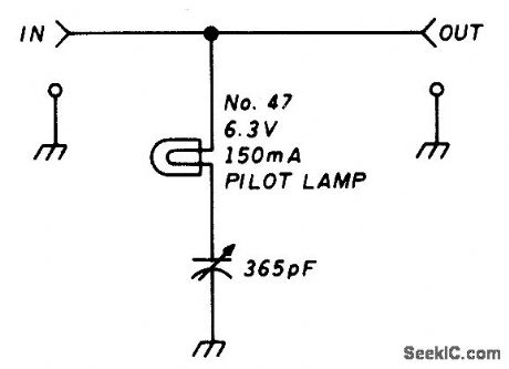
Relative power can be indicated with this simple circuit.Adjust the 365-pF variable capacitor fordesired lamp brightness. (View)
View full Circuit Diagram | Comments | Reading(786)
1_Hz_TO_10_MHz_VOLTAGE_TO_FREQUENCY_CONVERTER
Published:2009/7/9 5:35:00 Author:May

View full Circuit Diagram | Comments | Reading(966)
ON_INDICATOR
Published:2009/7/9 5:32:00 Author:May
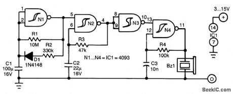
Battery-operated equipment can work on one set of batteries for a long time nowadays. However, if it is left on inadvertently, that long time is over very quickly. Moreover, flat (dead) batteries are always found at the wrong moment. The circuit proposed here is a sort of aide-memoire. Every two minutes, it emits 5 to 10 pips to indicate that the equipment is still switched on.
Basically, the circuit consists of three rectangle-wave generators and an inverter. The first of the gen-erators is formed by N1 and provides a signal with a period of about two minutes and a pulse duration of around 10 seconds. During those 10 seconds, the second generator starts operating in a one-second rhythm. Thus, N2 outputs 10 pulses every 2 minutes. That output is inverted so that N4, like N2, can only be enabled during the 10-second pulse train from N1. The difference is that during those 10 seconds, N4 is enabled and inhibited 10 times; this is what causes the pips.
Do not take the times and number of pulses too literally, because wide variances are between ICs from different manufacturers. On the other hand, component values are not critical, so it is fairly easy to adapt the circuit to personal taste or requirements. The buzzer can be a standard Toko type or equivalent.The current drawn by the circuit is negligible. (View)
View full Circuit Diagram | Comments | Reading(805)
MAINS_FAILURE_INDICATOR
Published:2009/7/9 5:30:00 Author:May
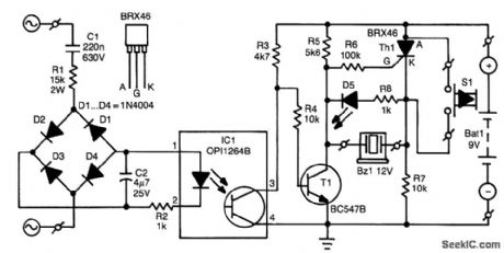
When the mains voltage is present at the input terminals, the transistor in the optocoupler is on, T1 is off, and silicon-controlled rectifier Th1 is in the conducting state. Because both terminals of the piezoelec-tric buzzer are then at the same potential, the buzzer is inactive. If the mains voltage drops out, transistor T1 conducts and causes one of the terminals of the buzzer to be connected to earth; the thyristor remains in the conducting state. In this situation, a large enough potential difference is across both the buzzer and D5 to cause these elements to indicate the mains failure-both audibly and visibly.
When the mains is restored, the circuit returns to its original state. A touch on the reset button then interrupts the current through the SCR so that the thyristor goes into the blocking state, and the other terminal of the buzzer is connected to ground.
The unit is powered by a 9-V battery and draws a quiescent current of 1.7-2.5 mA. It is important for the enclosure to be well-insulated.
If by accident the circuit to the optocoupler and R2 is broken, electrolytic capacitor C2 might be dam-aged because it will be charged well above its 25-V rating. Secondly, where a plug is used for the mains connection, it is advisable to solder a 1-MΩ resistor across C1 so that this capacitor does not retain its charge after the plug is removed from the mains socket. (View)
View full Circuit Diagram | Comments | Reading(2682)
BALANCE_INDICATOR
Published:2009/7/9 5:26:00 Author:May
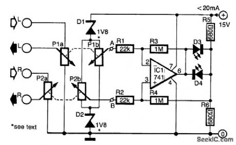
If your amplifier is fitted with two level controls, it actually offers you a balance control and a level control. A drawback of this is that it is quite difficult to set the balance properly. This can be obviated, however, by replacing the two monopotentiometers with stereo versions P1 and P2 in the diagram.
One half of the pair, P1A and P2A, assumes the tasks of the removed components. The other half is connected in a bridge circuit. The voltage between wipers of the potentiometers is then a measure of the balance between the two channels. The lower the potential, the better the balance. If you are interested in knowing the degree of unbalance, connect a center-zero moving coil meter with a bias resistor between A and B. With this arrangenient, zener diodes Dl and D2 can be omitted: they are necessary only with the LED indicator shown in the diagram to prevent the input voltage of the op amp from getting too close to the level of the supply voltage.
The circuit around IC1 is a classical differential amplifier. Resistors R5 and R6 provide a virtual earth for the LEDs, which is necessary to ensure that, in spite of the asymmetrical supply voltage, a positive and a negative output is obtained.
Because the LEDs have been included in the feedback loop of the indicator, the circuit is pretty sensi-tive. At only 40 mV, that is, just 1/400 of the supply voltage, one of the LEDs begins to light. The maximum current drawn by the LEDs is determined by the values of R5 and R6. (View)
View full Circuit Diagram | Comments | Reading(865)
| Pages:42/72 At 204142434445464748495051525354555657585960Under 20 |
Circuit Categories
power supply circuit
Amplifier Circuit
Basic Circuit
LED and Light Circuit
Sensor Circuit
Signal Processing
Electrical Equipment Circuit
Control Circuit
Remote Control Circuit
A/D-D/A Converter Circuit
Audio Circuit
Measuring and Test Circuit
Communication Circuit
Computer-Related Circuit
555 Circuit
Automotive Circuit
Repairing Circuit