
Audio Circuit
Index 13
LA4230/4250 8W Audio power amplifier circuit diagram
Published:2011/8/12 4:24:00 Author:Rebekka | Keyword: 8W, Audio power amplifier
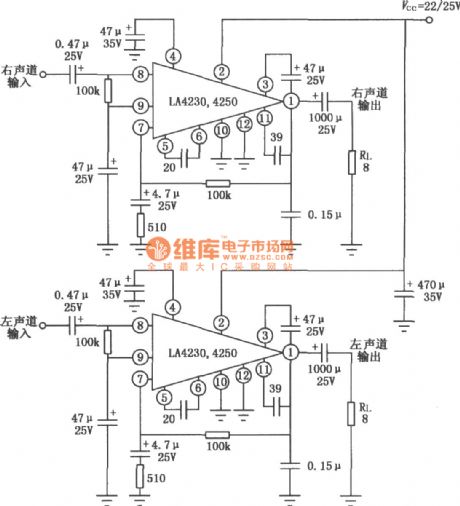
LA4230/4250 is 8W audio power amplifier. The output powers are 6W and 8W. It contains elimination ripple circuit and protection circuit inside. LA4230/4250 8W Audio power amplifier circuit diagram is shown as below.
(View)
View full Circuit Diagram | Comments | Reading(2318)
M22K Pioneer power amplifier circuit diagram
Published:2011/8/9 2:26:00 Author:Rebekka | Keyword: Pioneer, power amplifier
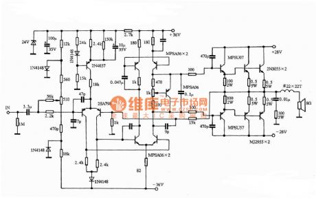
View full Circuit Diagram | Comments | Reading(7235)
Front Mark Levisin JC-2 circuit diagram
Published:2011/8/11 2:03:00 Author:Rebekka | Keyword: Front Mark Levisin
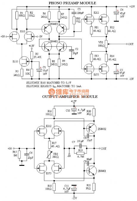
Front Mark Levisin JC-2 circuit diagram is shown as below.
(View)
View full Circuit Diagram | Comments | Reading(2578)
LM3886 BTL PA circuit diagram
Published:2011/8/11 2:03:00 Author:Rebekka | Keyword: BTL PA
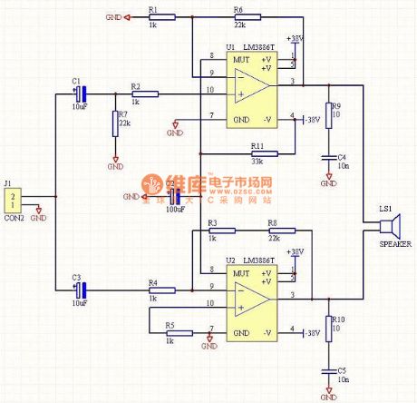
LM3886 BTL PA circuit diagram is shown as below.
(View)
View full Circuit Diagram | Comments | Reading(4367)
V.A.L VAA-70 push-pull tube amplifier circuit diagram
Published:2011/8/11 2:03:00 Author:Rebekka | Keyword: V.A.L , push-pull tube amplifier
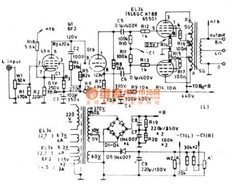
V.A.L VAA-70 push-pull tube amplifier circuit diagram is shown as below.
(View)
View full Circuit Diagram | Comments | Reading(2971)
LM4808 typical circuit diagram for two-channel headphone amplifier
Published:2011/8/16 21:49:00 Author:Rebekka | Keyword: two-channel headph amplifier
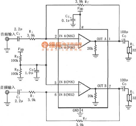
Figure shows the LM4808 for dual-channel amplifier typical circuit. Left and right channel audio signals are inputed LM4808 2, 6 feet respectively. After being amplified by internal amplifier, then they will be output by the foot 1, 7 respectively. The coupling capacitor Co isadded to the speaker. Amplifier gain is determined by resistors Ri and Rf, Av = Rf / Ri. The maximum power is PDMAX=VDD2/2π2RL. The LM4808 packaging has two amplifiers, so the total power consumption should be multiplied by 2.It is applied in a large temperature rangeenvironment , LM4808 does not install the heat sink. External input resistors and capacitors determine the input-3dB bandwidth: Input-3dB bandwidth fi-3db = 1/2πRiCi; Output-3dB bandwidth fo-3dB = 1/2πRLCo.
(View)
View full Circuit Diagram | Comments | Reading(2944)
LM4910 For two-channel amplifier typical circuit diagram
Published:2011/8/16 22:18:00 Author:Rebekka | Keyword: two-channel amplifier
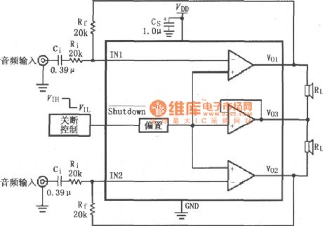
Figure shows the LM4910 for dual-channel amplifier typical circuit. Left and right channel audio signals are inputed LM4910 (MSOP / SO packaging) 1,2 feet respectively. After being amplified by internal amplifier, then they will be outputed by the foot 8, 7, 6 respectively and added to each speaker channel directly. Amplifier gain Av =- Rf / Ri, the maximum poweris PDMAX = 4VDD2/π2RL. External input resistors and capacitors determine the input-3dB bandwidth, taking Ci ≥ 1 / (2π × 20kΩ × 20Hz) with approximately 0.39μF capacitor. LM4910's pin 3 isconnect shutdown control outside.It is allowed to work when the 3 feet connect VDD (high level); It is not allowed to work when the 3 pin connect ground (low).
(View)
View full Circuit Diagram | Comments | Reading(1346)
LM4910 minimum output noise / reduce output power circuit diagram
Published:2011/8/16 22:17:00 Author:Rebekka | Keyword: minimum output noise , reduce output power

The figure shows the LM4910's minimum output noise / reduce the output power circuit. Measures to reduce the output noise are: it adds a resistor Rseries in series between the output and the load to reduce the output noise and achieve the purpose of reducing noise. The two ends of feedback resistance Rf are connected ahigh frequency bypass capacitor Cf in parallelis for keeping down high-frequency noise. J1 is a shorted jumper. The amplifier is in shutdown mode and power consumption is minimum when J1 short jumper is earthing. When J1 short jumper is off(VDD high level), the amplifier is in working mode and the power dissipation is PDMAX=4VDD2/π2RL.
(View)
View full Circuit Diagram | Comments | Reading(1339)
LMV1012-07/15/25 High gain microphone amplifier circuit diagram
Published:2011/8/16 22:25:00 Author:Rebekka | Keyword: High gain , microphone amplifier
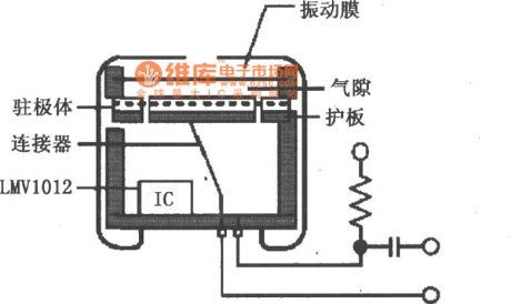
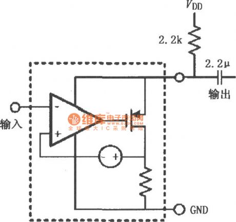
LMV1012 is a small electret microphone audio amplifier series, which is mainly used to replace the widely used JFET amplifier. LMV1012 seriesareused for adapting to the environmental site or RF noise that requires signal integrity requirements for applications, such as cellular communications systems, PDA's, car accessories etc. It guarantees 2.2 ~ 5.0V operating voltage range, the fixed gain of 7.8dB, 15.6dB and 23.8dB. Relative to the JFET amplifier, LMV1012 series amplifier has excellent gain accuracy and temperature stability. LMV1012 series can be used for two foot small electret microphone, direct pin to pin compatible JFET microphone on the market today. The device provides two 4-bump micro SMDTM package, LMV1012TP-07、LMV1012TP-15、LMV1012TP-25 pot package 1.8mm thickness, LMV1012UP-25 pot package 1.3mm thickness. It is applicable to most small electret condenser microphone.
The pinout of LMV1012 is shown as below.
Internal circuit:
(View)
View full Circuit Diagram | Comments | Reading(2074)
10W Audio power amplifier TDA2006 typical application circuit diagram
Published:2011/8/16 22:23:00 Author:Rebekka | Keyword: 10W Audio power amplifier, typical application
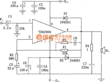
10W Audio power amplifier TDA2006's typical application circuit diagram is shown as below.
(View)
View full Circuit Diagram | Comments | Reading(5990)
20W Hi—Fi Audio power amplifier TDA2020 BTL application circuit diagram
Published:2011/8/16 22:23:00 Author:Rebekka | Keyword: 20W Hi—Fi, Audio power amplifier , BTL application
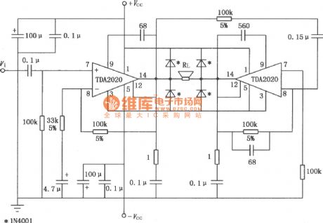
20W Hi—Fi Audio power amplifier TDA2020's BTL application circuit diagram is shown as below.
(View)
View full Circuit Diagram | Comments | Reading(3890)
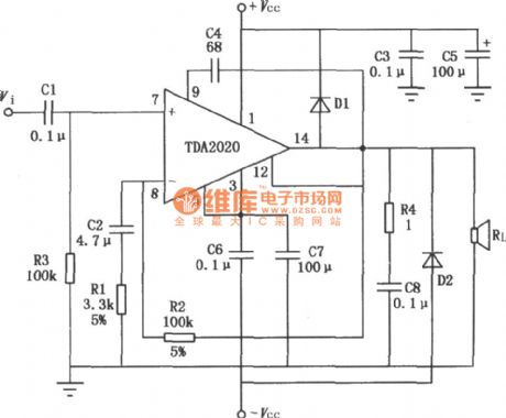
Typical application circuit diagram of 20W Hi—Fi audio power amplifier TDA2020
Published:2011/8/17 1:27:00 Author:Rebekka | Keyword: 20W Hi—Fi, Audio power amplifier , typical application
View full Circuit Diagram | Comments | Reading(3171)
BTL application circuit diagram of TDA2030A audio power amplifier
Published:2011/8/17 2:25:00 Author:Rebekka | Keyword: Audio power amplifier , BTL application
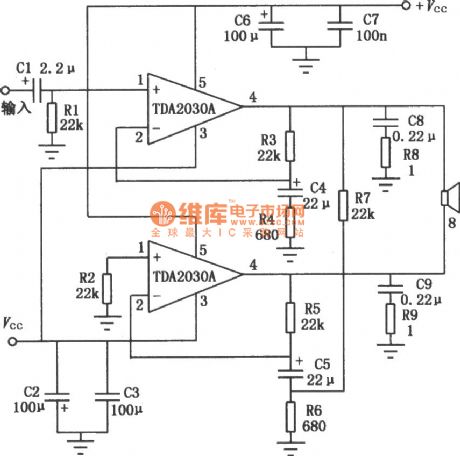
View full Circuit Diagram | Comments | Reading(7055)
Low Noise 200MHZ Broadband Amplifier Circuit
Published:2011/8/1 5:38:00 Author:Sue | Keyword: Low Noise, Broadband, Amplifier
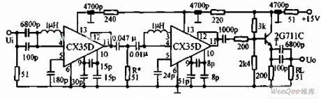
The circuit consists of two CX35D. The main technological indicators are: bandwidth of 10-20MHz; When the load resistance value is 500Ω, the voltage gain Au is not less than 80; the undistorted output voltage is not less than 500mV; the short noise which is put on input terminal is less than 40μV. When the capacitors which are connected to pin5,pin9,pin10 are adjusted, the band width can reach 300KHz; Every level should be shielded;Transistor's characteristic frequency should be larger than 1000MHz. (View)
View full Circuit Diagram | Comments | Reading(1091)
Please-Close-the-Door Language Integrated Circuit
Published:2011/7/21 21:59:00 Author:Joyce | Keyword: Please Close the Door, Language , Integrated
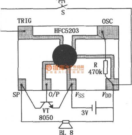
HFC5203A is large-scale CMOS integrated circuit, storing a female voice please close the door . The pronunciation is clear and the peripheral circuit is simple. With level and do-not-keep- triggering mode, it can be widely used in banks, stores, security departments, air conditioning rooms and electric refrigerators to give reminders. The typical application circuit of HFC5203A is as shown in the figure.
(View)
View full Circuit Diagram | Comments | Reading(1603)
Back-up-Attention-Please Language Integrated Circuit
Published:2011/7/21 22:00:00 Author:Joyce | Keyword: Back up, Attention Please , Language , Integrated
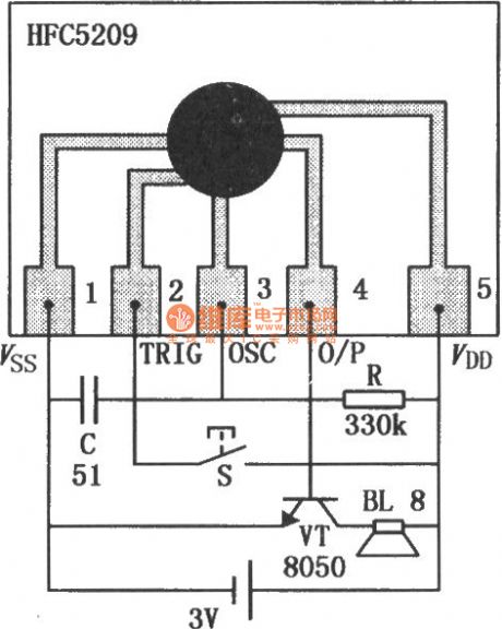
HFC5210 can send out warning —— back up, attention please .This circuit has good performance, clear pronunciation and a simple peripheral circuit. It is one of the most commonly used warning circuits for backing up. Its typical application circuit is as shown in the figure. (View)
View full Circuit Diagram | Comments | Reading(1080)
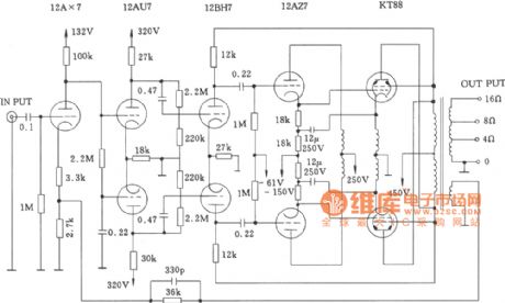
McIntosh Power Amplifier MC-275 Circuit
Published:2011/8/6 8:47:00 Author:Felicity | Keyword: McIntosh, Power Amplifier
View full Circuit Diagram | Comments | Reading(5738)
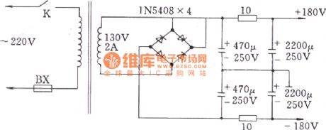
OTL Amplifier Power Current Circuit (For Tube Amp)
Published:2011/8/6 8:49:00 Author:Felicity | Keyword: OTL, Amplifier Power, Current Circuit, Tube Amp
View full Circuit Diagram | Comments | Reading(1906)
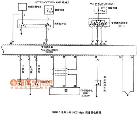
BMW7 Series A5S 560Z 88pin Transmission Circuit (the 2nd)
Published:2011/8/6 8:49:00 Author:Felicity | Keyword: BMW7 Series, 88pin, Transmission Circuit, (the 2nd)
View full Circuit Diagram | Comments | Reading(890)
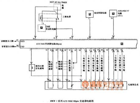
BMW7 Series A5S 560Z 88pin Transmission Circuit (the 1st)
Published:2011/8/8 21:41:00 Author:Felicity | Keyword: BMW7 Series, 88pin, Transmission Circuit
View full Circuit Diagram | Comments | Reading(1217)
| Pages:13/54 1234567891011121314151617181920Under 20 |
Circuit Categories
power supply circuit
Amplifier Circuit
Basic Circuit
LED and Light Circuit
Sensor Circuit
Signal Processing
Electrical Equipment Circuit
Control Circuit
Remote Control Circuit
A/D-D/A Converter Circuit
Audio Circuit
Measuring and Test Circuit
Communication Circuit
Computer-Related Circuit
555 Circuit
Automotive Circuit
Repairing Circuit