
Audio Circuit
Index 15
50_W_TWO_STAGE_OUTPUT
Published:2009/7/15 2:54:00 Author:Jessie
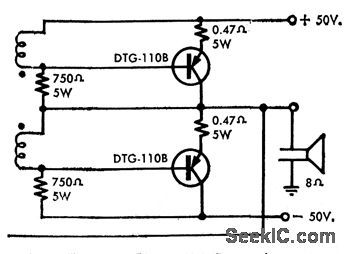
Produces over 50-w rms audio power and has simple drive requirements.-High-Power Nu-Base Germanium Transistors (Delco Radio ad), Electronics, 39:7, p 20-21. (View)
View full Circuit Diagram | Comments | Reading(1488)
NPN_PHONO_PREAMP
Published:2009/7/15 2:53:00 Author:Jessie
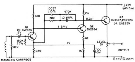
Input of 6 mv at 1 kc from magnetic cartridge gives 1 v output, which is 15 db below clipping level and 72 db above unweighted noise level. RIAA equalized output is within 1 db from 40 cps to 12 kc.- Transistor Manual, Seventh Edition, General Electric Co., 1964, p 257. (View)
View full Circuit Diagram | Comments | Reading(3047)
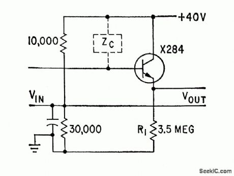
500_MEG_D_C_INPUT_RESISTANCE
Published:2009/7/15 2:45:00 Author:Jessie
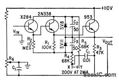
Bootstrap-collector circuit uses starved transistor to provide 500-meg d-c input resistance with 100-v input signal. A-c resistance is even higher, in the 1,000-megohm region at low audio frequencies.-B. M.Bramson, Starved Transistors Raise D-C Input Resistance, Electronics, 32:5, p 54-55. (View)
View full Circuit Diagram | Comments | Reading(1080)
REDUCING_ODD_HARMONIC_DISTORTION
Published:2009/7/15 2:44:00 Author:Jessie
Grid-plate transfer characteristic of class-B amplifier is linearized to eliminate harsh odd-harmonic distortion, through use of compensation network having nonlinear transfer function. Distortion is cut to 2.6% at 16 w output.-B. Sklar, Reducing Distortion in Class.B Amplifiers, Electronics, 32:21, p 54-56. (View)
View full Circuit Diagram | Comments | Reading(1319)
DARLINGTON_WITH_VOLTAGE_DIVIDER
Published:2009/7/15 2:42:00 Author:Jessie
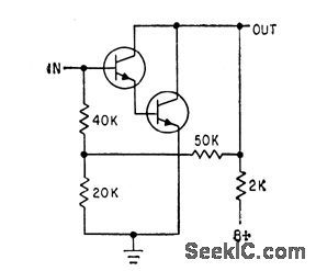
Additional resistors in voltage divider reduce bias voltage, to simplify manufacture as integrated circuit. Useful up to 100 kc.-L.Pollock and R. Gutteridge, Latest Design Techniques for Linear Microcircuits, Electronics, 35:41, p 47-49. (View)
View full Circuit Diagram | Comments | Reading(1145)
45_W_A_F_OUTPUT
Published:2009/7/15 2:40:00 Author:Jessie
Operates with convection cooling over temperature range of -10 to +50℃. Forward voltage drop of diodes decreases with increasing temperature, to hold emitter currents essentially constant. Uses quasi complementary symmetry.-M. B. Herscher, Designing Transistor A.F Power Amplifiers, Electronics, 31:15, p 96-99. (View)
View full Circuit Diagram | Comments | Reading(2396)
SYNTHETIC_PUSH_PULL
Published:2009/7/15 2:29:00 Author:Jessie
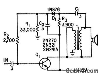
Single transistor in sliding class-A output requires no input transformer, while approximating push-pull class-B output stage.-J. A. Worcester, One. Transistor Push-Pull, Electronics, 32:24, p 74. (View)
View full Circuit Diagram | Comments | Reading(1237)
100_350_CPS_RECEIVER
Published:2009/7/15 2:28:00 Author:Jessie
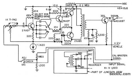
Input signal from electrodes of crevasse detector is attenuated to suitable level at constant impedance of 1,000 ohms by T-pad and passed to 2N107 preamplifier whose supply voltage is stabilized at 5.8 v by reversed 71620 silicon diode shunt operating at zener point. Signal is then fed through bandpass L-C filter to amplifier, driver, and final 355 class A stage that drives recorder pen motor and relaymeler.-H. P. Van Eckhardt, Crevasse Detector Blazes Glacial Trails, Electronics, 31:3, p 63-65. (View)
View full Circuit Diagram | Comments | Reading(1138)
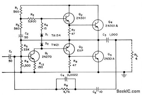
CLASS_AB_PUSH_PULL_AUDIO
Published:2009/7/15 2:14:00 Author:Jessie
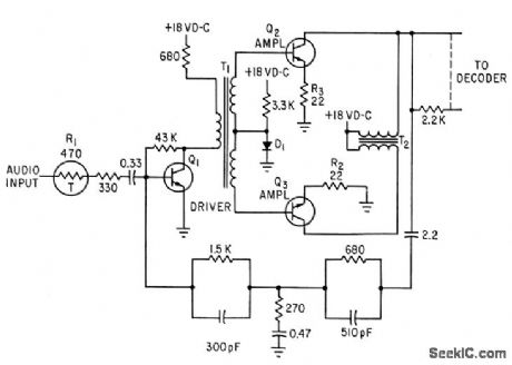
Sensistor R1 in a-c coupled driver compensates for effects of temperature on amplifier gain on amplifier gain. Negative feedback stabilizesfrequency and phase response. Circuit drives 20 decoders in Mercury spacecraftcommand receiver.-R. Elliott, First Details on Mercury Spacecraft Command Receiver,Electronics, 36;5, p 32-35. (View)
View full Circuit Diagram | Comments | Reading(964)
STABILIZED_MULTI_INPUT_AUDIO_PREAMP
Published:2009/7/15 2:07:00 Author:Jessie
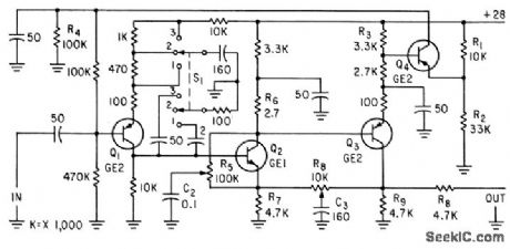

Switch gives choice of input impedance, frequency response, and level-compensation network. R5 is tone control. Q4 Provides biascurrent to base of Q1 for stabilization-H.W. Parmer, Two Easy Ways to Stabilize Power -Transistor Hi-fi Amplifiers, Electronics,35:43,p 56-58. (View)
View full Circuit Diagram | Comments | Reading(1042)
FET_OUTPUT_STAGE
Published:2009/7/15 2:56:00 Author:Jessie
Bootstrapped input, Darlington driver, and White follower give voltage gain of one, input impedance of 1 meg, and output impedance of 10 ohms.-B. Smifh, Low-Noise FETs Sound Good To Circuit Designers, Electronics, 37:31, p 58-62. (View)
View full Circuit Diagram | Comments | Reading(1227)
120_150_MHz_FOR_TRANSISTOR_RADIO
Published:2009/7/15 5:02:00 Author:Jessie
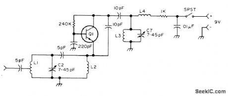
Values shown cover bands for aircraft radio, 2-m amateur radio band, and other services. Circuit is regenerative converter, with incoming signal tuned by La-C2 and mixed in 2N2222 or equivalent transistor connected as oscillator with frequency controlled by L3 and C7. Difference frequency is adjusted to fall in standard broadcast band, for pickup by radio when converter is mounted close to ferrite loop. For local stations, antenna of converter can be 19-in length of wire. L2 and L4 are 100-μH chokes or about 20 in of fine wire wound on 100K resistor. -S. Kelly, Simple VHF Monitor, 73 Magazine, July 1976, p160. (View)
View full Circuit Diagram | Comments | Reading(2622)
ADJUSTABLE_SQUARE_WAVES
Published:2009/7/15 4:57:00 Author:Jessie
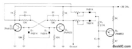
Q1 and Q2 form flip-flop, with UJT Q3 connected as time delay. When power is applied, one flip-flop transistor conducts and C1 charges through one pot and diode. When C1 reaches firing voltage of UJT, it conducts and resulting output pulse triggers flip-flop, Sequence of events now repeats, with C1 charging through other diode. By proper selection of C1 and pot values, circuit becomes square-wave generator with each pot controlling duration of one half-cycle. With one pot replaced by fixed resistor, circuit becomes pulse generator with other pot controlling pulse-repetition rate. If equal-value fixed resistors replace pots and R1 is changed to pot, circuit becomes symmetrical square-wave generator with pot controlling frequency,-I. Math, Math's Notes, CQ, April 1974, p 64-65 and 91-92. (View)
View full Circuit Diagram | Comments | Reading(1160)
20_W_SINGLE_ENDED_PUSH_PULL_OUTPUT
Published:2009/7/14 4:10:00 Author:May
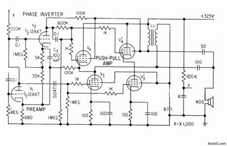


Doubling number of output power tubes doubles ower output and halves loudspeaker impedance requirement. Separate cathode R-Cassembly for each pair of output tubes is recommended, but only one double choke isrequired. All pentodes are 6CW5.-J.Rodrigues De Miranda, Push-Pull Amplifiers DriveSpeaker Directly, Electronics, 31:29, p 76-79. (View)
View full Circuit Diagram | Comments | Reading(1565)
100_MEG_INPUT_RESISTANCE
Published:2009/7/14 4:08:00 Author:May
High d-c input resistance is obtained with grounded-collector circuit operating under starved conditions. A-c input impedances of 100 megare obtain-able at audio frequencies, as required for photoconductive devices.-B. M.Bramson, Starved Transistors Raise D-C Input Resistance, Electronics, 32:5, p 54-55. (View)
View full Circuit Diagram | Comments | Reading(1037)
2_STAGE_R_C_COUPLED_AUDIO_AMPLIFIER
Published:2009/7/14 4:07:00 Author:May
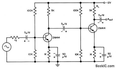
Input impedance for basic circuit is about 1300 hms. Design equations are given.- Transistor Manual, Seventh Edition, General lectric Co., 1964, p 242. (View)
View full Circuit Diagram | Comments | Reading(2380)
RING_COUNTER_USES_GATE_TURNOFFS
Published:2009/7/14 3:54:00 Author:May
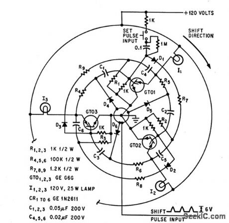
Closing of set pulse input switch turns on first gto. Applying voltage to its lam load. Each shift pulse input then transfers conduction to next gto and lamp.-D.R. Grafham. Now the Gate Turnoff Switch Speeds up D-C Switching Electronics.37:12,p64-71 (View)
View full Circuit Diagram | Comments | Reading(1048)
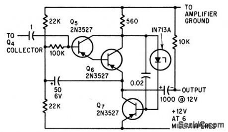
DRIVER_FOR_FADIRA
Published:2009/7/14 3:54:00 Author:May
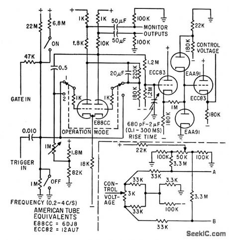
can be operated either in free-funning mode or in triggered orgated mode to produce Control voltage that will drive electronic fader. Correction network at lower right transfers control voltage to fader and minimizes switchingtransient.-E .de Boer, Electronics, Fader for Auditory Research,Electronics, 33:50,p 85-87. (View)
View full Circuit Diagram | Comments | Reading(1017)
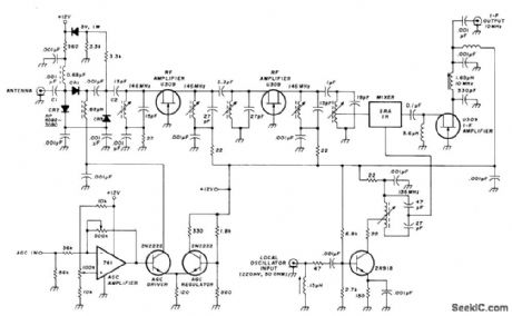
144_MHz_TO_28_MHz
Published:2009/7/15 5:22:00 Author:Jessie
Brings 2-meter band to input range of ordinary amateur receiver. Crystal eliminates need for multiplier stages that can generate spurious responses. Signal can be injected from external source if crystal is re moved. -Construction Hints for VHF Converters, QST, Sept. 1975, p 32-33 and 39. (View)
View full Circuit Diagram | Comments | Reading(1777)
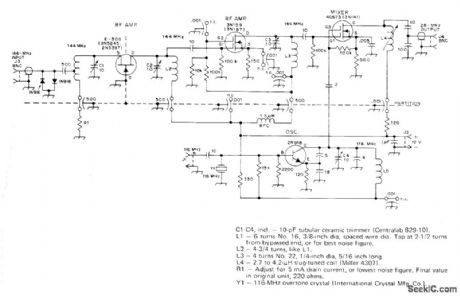
2_METER_FOR_10_MHz_IF
Published:2009/7/15 5:20:00 Author:Jessie
Designed for extreme linearity and selectivity while keeping noise figure below 5 dB Circuit has +15 dBm intercept point and 16-dB power gain, Five tuned circuits at input frequency give overall bandwidth of 4 MHz, with image suppression of 60 dB for 10-MHz IF and 80 dB for 30-MHz IF. Converter uses grounded-gate FET circuit. -U. Rohde, High Dynamic Range Two-Meter Converter, Ham Radio, July 1977,p55-57.
(View)
View full Circuit Diagram | Comments | Reading(1486)
| Pages:15/54 1234567891011121314151617181920Under 20 |
Circuit Categories
power supply circuit
Amplifier Circuit
Basic Circuit
LED and Light Circuit
Sensor Circuit
Signal Processing
Electrical Equipment Circuit
Control Circuit
Remote Control Circuit
A/D-D/A Converter Circuit
Audio Circuit
Measuring and Test Circuit
Communication Circuit
Computer-Related Circuit
555 Circuit
Automotive Circuit
Repairing Circuit