
Audio Circuit
Index 10
4 microphones mixer circuit with TL081
Published:2012/9/10 21:17:00 Author:Ecco | Keyword: 4 microphones, mixer
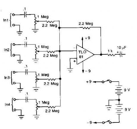
A TL081 op amp is used as a high impedance to low. converter and a signal mixer. The input impedance is about 1 megohm and the output impedance is about 1 kohm. Two 9 volt batteries are used as power source. (View)
View full Circuit Diagram | Comments | Reading(7789)
Pushbutton Activated Service Request Beeper
Published:2012/9/4 20:24:00 Author:Ecco | Keyword: Pushbutton , Activated, Service Request, Beeper
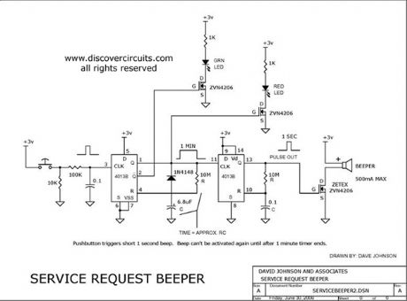
A single press of a pushbutton switch turns on a beeper for one second but can?t be activated again for 60 seconds.
Source: discovercircuits (View)
View full Circuit Diagram | Comments | Reading(1)
AUDIO FREQUENCY DIGITAL NOISE GENERATOR
Published:2012/9/4 20:13:00 Author:Ecco | Keyword: AUDIO , FREQUENCY , DIGITAL , NOISE GENERATOR

When you need to test an audio circuit with broadband noise, this circuit works great. It uses just three inexpensive C-MOS ICs that generate a series of output pulses whose widths vary randomly. I included a level control pot.
Source: discovercircuits
(View)
View full Circuit Diagram | Comments | Reading(1)
True Stereo Indicator Detects L-R Signal Difference
Published:2012/9/3 1:32:00 Author:Ecco | Keyword: True , Stereo , Indicator, Detects , L-R Signal Difference
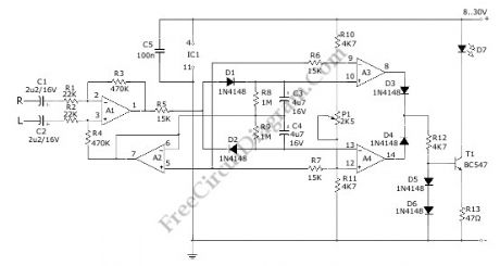
Source: freecircuitdiagram
This true stereo indicator is different from what we usually find on FM radio receiver, which is usually a pilot tone detector. A stereo broadcast from FM radio station contain pilot tone, but a presence of pilot tone doesn’t necessarily a stereo broadcast signal since a mono FM transmitter ca broadcast pilot tone as well. Since this circuit detect the difference between left and right channel, this circuit can detect a real stereophonic programs. When there is no difference between R and L input signals, the output A1 and output A2 is at the same potential. That will make a a virtual ground rail at half the supply voltage. Here is the schematic diagram of the circuit:
(View)
View full Circuit Diagram | Comments | Reading(1432)
Discrete Sliding Tone (Frequency Ramp) Doorbell
Published:2012/9/3 1:31:00 Author:Ecco | Keyword: Discrete Sliding Tone , Frequency Ramp, Doorbell

Source: freecircuitdiagram
This doorbell circuit produces a low tone that will slide up to higher frequency. The equivalent total resistance connected between the base of Q1 and ground (Rbg) , and coupling capacitor C1 determines the AF oscillator’s frequency. The resistance (Rbg) is equal to (R2+R1)R3. Here is the schematic diagram of the circuit:
(View)
View full Circuit Diagram | Comments | Reading(1095)
TDA7056 3W BTL Mono Audio Power Amplifier
Published:2012/9/3 1:27:00 Author:Ecco | Keyword: 3W , BTL , Mono , Audio , Power Amplifier
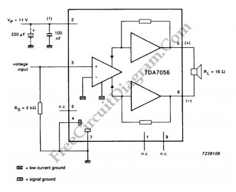
Source: freecircuitdiagram
For mono output amplifier application, TDA7056 IC can be your option. Compact but powerful, this integrated circuit is contained in a 9 pin medium power package. This device is designed for battery fed portable equipments such as mono recorders, radios and television. To attract the market, TDA7056 has many features such as low power consumption. For more reliable operation, TDA7056 also has short circuit proof and ESD (Electro Static Discharge) protected on all pins. Designing application with this IC should be easy since no external components is needed. To make sure you’ll love this chip, this device also has no switch on/off clicks. Overall, TDA7056 has good stability.
(View)
View full Circuit Diagram | Comments | Reading(2709)
Compressor Circuit with 570/571 Compandor IC
Published:2012/9/3 1:26:00 Author:Ecco | Keyword: Compressor, Compandor IC
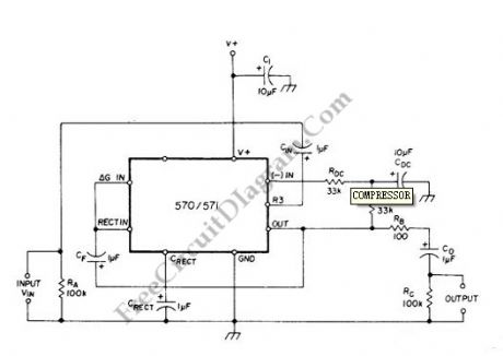
Source: freecircuitdiagram
Compressor circuit provide high gain for low amplitude input and provide low gain for high amplitude input. This action, in effect, produce a nearly constant amplitude even though the input has very high dynamic range (very high amplitude variation from time to time). The action of compression like this is needed in some situation, such as in maximizing modulation depth in broadcasting, or sustaining electric guitar signal which has very high variation between the plucking time and fading out. The following circuit has complementary input/output characteristic and unity gain at 0.775 VRMS input. Voltage gain through compressor is square root of 0.7/Vin. Vin is average input voltage. This circuit uses Signetics dual channel compandor IC. 570 has lower inherent distortion and higher supply voltage range (6-24 V) than 571 (6-18 V).
(View)
View full Circuit Diagram | Comments | Reading(2746)
Sound-Activated Lamp (Relay/Switch)
Published:2012/9/3 1:24:00 Author:Ecco | Keyword: Sound-Activated Lamp , Relay, Switch
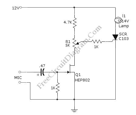
Source: freecircuitdiagram
This simple circuit shown int the schematic diagram actives the switch using sound. We can use this circuit for various applications, such as automatic (sound-controlled) disco light or car’s LED light show. The Q1 amplify the audio from mic. The R1 is used to adjust the peak of signal to greater than about 0.7 volts, act as sensitivity adjuster. A certain level, the signal coming from microphone, after amplification by Q1, will trigger the SCR and light lamp I1. If we change the lamp with a relay, then we can get a sound-activated relay/switch, which can be used to control more powerful / high wattage high voltage lamps. If we use a relay, place a 1N4007 diode in parallel with the relay coil to prevent the back-emf from relay coil destroying the SCR. Here is the schematic diagram of the circuit:
(View)
View full Circuit Diagram | Comments | Reading(0)
Basic Complementary (Push-Pull) Power Amplifier Circuit
Published:2012/9/3 1:19:00 Author:Ecco | Keyword: Basic Complementary, Push-Pull, Power Amplifier
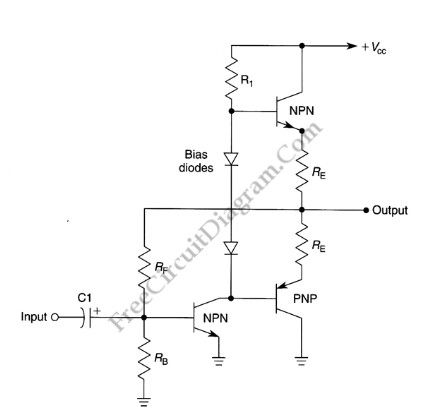
Source: freecircuitdiagram
This amplifier circuit is very popular audio power amplifier circuit type. We call it a complementary since the final transistors is an NPN-PNP pair, each with the same characteristics. This circuit produce an AB class amplifier, since each transistor works in slightly more than half cycle of the signal. There is overlap area when both transistor conduct a current, and this area will be around its stationary current (when the input signal is zero). This circuit is also known as push-pull amplifier circuit since each transistor in the pair is working alternatively. Here is the schematic diagram of the circuit:
(View)
View full Circuit Diagram | Comments | Reading(2678)
Voltage-Controlled Attenuator (Volume Control) Using FET
Published:2012/9/3 1:16:00 Author:Ecco | Keyword: Voltage-Controlled Attenuator , Volume Control, FET
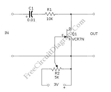

Using the circuit shown in the schematic diagram below, we can control the low-level audio signals with ±3V variable DC voltage. This attenuator circuit uses a field effect transistor (FET) to shunt the signal to ground. The R2 is used to control the output level (the attenuation level), but you can use other source of voltage signal to control the grid of the FET, such as DAC output, just remember that this voltage is a negative going signal (you can use with DAC which uses symmetric power supply system). The minimum output of this circuit is when gate bias is zero. When the gate bias is set close to pinchoff value, the circuit will produce maximum output with value that equal to input level. Here is the schematic diagram of the circuit:
Source: freecircuitdiagram (View)
View full Circuit Diagram | Comments | Reading(4684)
60-dB Range Compressor For Audio
Published:2012/9/3 1:13:00 Author:Ecco | Keyword: 60-dB Range, Compressor , Audio
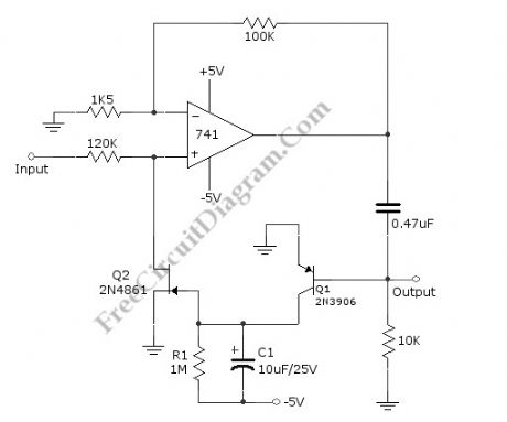
A compressor circuit shown in the schematic diagram below can produce consistent output of 1.4V P-P over entire 60dB range that is very useful for audio level/volume stabilization. As the main components, this circuit uses a 741 opamp and JFET. With input range of 20mV to 2oV, this circuit has delay time of 0.4s (decay time) and response time of 1.2ms (attack time). The JFET is used as voltage-controlled resistor in peak-detecting control loop of 741 opamp. Here is the schematic diagram of the circuit:
source: freecircuitdiagram (View)
View full Circuit Diagram | Comments | Reading(3424)
Telephone Circuit: Music On Hold
Published:2012/9/3 1:09:00 Author:Ecco | Keyword: Telephone , Music On Hold
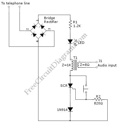
Waiting a call hold can be boring if there is only silence on the line. It’s a good thing to present an “easy music” in call hold, make a long waiting time feels much shorter. This simple circuit (consists of diodes, SCR, and some passive components) allows to place the caller on hold in one room then answer the phone again at another place, or at same phone at later time after doing something. This circuit is called music hold on circuit. This circuit will be turned off automatically when the phone is picked up the second time and the conversation can be continued. Here is the schematic diagram of the circuit:
Source: freecircuitdiagram (View)
View full Circuit Diagram | Comments | Reading(1)
Loud 10-W Car Alarm Siren
Published:2012/9/3 1:07:00 Author:Ecco | Keyword: Loud, 10-W, Car Alarm Siren

By generating square-wave output that sweeps down and up in frequency, this circuit can produce force field of high-intensity sound inside car. This circuit can make a car thieve panics and decide to run before anyone catch his action. D1, C1 and R1 produce triangle waveform by shaping a square wave output of IC1. If using sweeping alarm sound is prohibited by regulation, then C1 can be removed to provide legal two-tone sound. The diodes are general purpose small signal silicon except D2 which is silicon rectifier rated 1 A at 50 PIV. This circuit can handle up to 10W depends on the horn loudspeaker. Here is the schematic diagram of the circuit:
(View)
View full Circuit Diagram | Comments | Reading(2060)
Simple long-distance wireless microphone circuit
Published:2012/8/27 21:45:00 Author:Ecco | Keyword: Simple, long-distance, wireless microphone
The loop antenna L1 for emission also serves as the oscillation coil, the high frequency current flowing in antenna has the same resonance with the oscillation frequency, so it is always in the best emission state. In practice, the launching distance is about 100-1850M in empty area ( receivers is a the Pocket Radio TOLY1781, and the receiver distance of antenna is added as 0.8m ), in contrast, under the equivalent working voltage, current and emission frequency, if L1 is changed by an ordinary spiral circle, oscillation transistor collector is connected to a 5PF capacitor with a 0 . 8M trolley line, the two launching transmission distances are almost equivalent to prove that the concealed shaped antenna, which is also used as the oscillator coil, has a quite high emission efficiency.
(View)
View full Circuit Diagram | Comments | Reading(3588)
The stereo encoder circuit with discrete elements
Published:2012/8/27 22:15:00 Author:Ecco | Keyword: stereo encoder , discrete elements
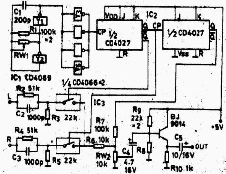
In the figure IC1-4069, Y1 and Y2 form a oscillator with frequency in 76KHZ; then the frequency is isolated and shaped by Y3-Y6 to be sent into frequency-halving circuit composed of IC2 and dual JK flip-flop CD4027, then it will produce a symmetrical + /-38KHZ and 19KHZ square wave, in which the + /-38KHZ square wave is used for controlling the IC3 analog switch CD4066; the stereo audio signal is input to switch for switching modulation, then it is mixed with 19KHZ frequency signal and sent to FM modulator after being isolated by the transistor 9014. FM modulator circuit can refer to a variety of FM transmitter circuits at the site.
(View)
View full Circuit Diagram | Comments | Reading(2158)
FM wireless headphone circuit
Published:2012/8/20 22:08:00 Author:Ecco | Keyword: FM , wireless headphone
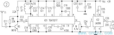
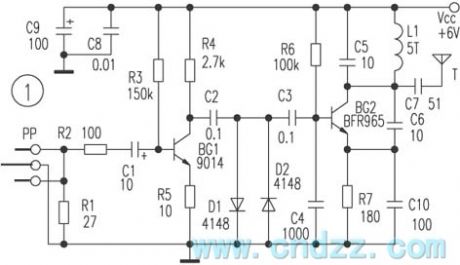
Figure 1 is a transmitting circuit of wireless headset, the audio signal obtained by television headphone jack bu passing stereo headphone plug is amplified by BG2, then it is amplitude limited by limiter circuit composed of D1, D2, C2, C3 and sent to high frequency oscillator composed of BG2; the modulated FM signal is coupled by C7 and emitted by antenna. Figure 2 is a receiving circuit which uses dedicated FM receiver module IC1 TDA7021T as the core. The demodulated audio signal is output from the foot sent to IC2 LM386 for power amplification and promote the headphones sound. Transistor BG 9018 form the high - frequency amplifier stage in order to improve the reception sensitivity.
(View)
View full Circuit Diagram | Comments | Reading(4441)
Medium-wave AM radio circuit
Published:2012/8/19 21:28:00 Author:Ecco | Keyword: Medium-wave , AM , radio
This circuit uses a FET for the preamp, and input signal is applied to the gate. In the drain loops, two loops have band-pass filter, and they use two tunable diodes for tuning. The resonant circuit determines the frequency, which is connected to pin 10 and 11 of IC.
(View)
View full Circuit Diagram | Comments | Reading(1872)
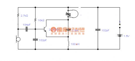
The production circuit of three-tube FM wireless microphone
Published:2012/8/20 20:11:00 Author:Ecco | Keyword: three-tube , FM, wireless microphone
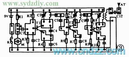
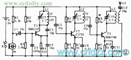
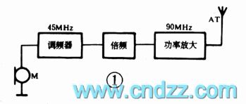
The microphone uses the direct FM mode with the center frequency in 90MHz, transmit power is about 0.5W, and the largest frequency offset is 50kHz, and the transmitting distance is not less than 50 meters. The block diagram and schematic diagram are shown in Figure 1,2. The audio signal generated by the electret microphone acts on the emission junction of the modulator T1 as the modulation voltage. The size of voltage directly changes the junction capacitance of the transistor emitter junction, and the junction capacitance is a part of the circuit parameters; fo is about 45MHz, and the output frequency can be up to 90MHz after frequency doubling, the FM signal is emitted by an antenna after being amplified by high-frequency amplifier.
(View)
View full Circuit Diagram | Comments | Reading(1837)
FM wireless microphone circuit with voltage regulator circuit
Published:2012/8/21 1:53:00 Author:Ecco | Keyword: FM , wireless microphone , voltage regulator
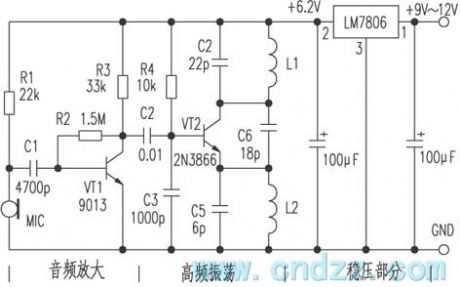
The circuit consists of three parts: 1 . Audio amplifier section; 2 . High-frequency oscillation part; 3 . Regulators parts. The signal is sent into a base of the transistor VT1 from the microphone MIC, then it is coupled to the base of high-frequency oscillation circuit VT2 by C2 after being amplified by VT1, then it is emitted by antenna. The working frequency of this circuit is between 85 ~ 104MHz. MIC selects high-sensitivity electret microphone, VT1 uses 9013H with β ≥ 125. VT2 is 2N3866 with β ≥ 90, L1, L2 use∮ 0.71mm enameled wires with four turns and 10 turns around ordinary pen core, C4, C5, C6 use ceramic capacitors, error is ± 5 % . The three-terminal regulator uses the LM7806 power supply with 9V battery, and the circuit board can be made by yourself.
(View)
View full Circuit Diagram | Comments | Reading(3020)
Audio amplifier circuit diagram composed of TDA1013
Published:2011/10/18 3:06:00 Author:Rebekka | Keyword: Audio amplifier

TDA1013 function and reference voltage Pin 1: 0V - to Pin 2: 7.7V-- audio outputPin 3: 16V - Power Pin 4: 13.5V-- Power Supply Pin 5: 0.3V-- Amplifier Input Pin 6: 6.7V-pre-outputPin 7: 2.8V-- Volume Control Pin 8: 1.9V-audio inputPin 9: 0V-ground (View)
View full Circuit Diagram | Comments | Reading(11230)
| Pages:10/54 1234567891011121314151617181920Under 20 |
Circuit Categories
power supply circuit
Amplifier Circuit
Basic Circuit
LED and Light Circuit
Sensor Circuit
Signal Processing
Electrical Equipment Circuit
Control Circuit
Remote Control Circuit
A/D-D/A Converter Circuit
Audio Circuit
Measuring and Test Circuit
Communication Circuit
Computer-Related Circuit
555 Circuit
Automotive Circuit
Repairing Circuit