
Audio Circuit
Index 19
GATED_AMPLIFIER_DRIVES_FERRITE_CORES
Published:2009/7/20 1:24:00 Author:Jessie
Used in shockproof recorder in which each amplifier drives a line of six cores. Interrogation of cores releases stored information for processing.-C. P. Hedges, Digital Recorder Holds Data After Shock, Electronics, 32:12, p 60-62. (View)
View full Circuit Diagram | Comments | Reading(1112)
SATELLITE_RECORDER_AND_TRANSMITTER
Published:2009/7/20 1:16:00 Author:Jessie
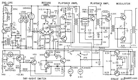
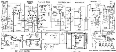
Primary video signal bandwidth is 0 to 240 cps. Direct-record system uses 290-cps sub carrier for reproducing d-c component of signal, giving 50-cps lower sideband. Upper sideband (530 cps) is suppressed. Transmitter uses crystal-controlled 108-Mc Hartley oscillator, feeding 1 w to antenna.-R. Hanel et al, Tracking Earth's Weather with Cloud-Cover Satellites, Electronics, 32:18, p 44-49. (View)
View full Circuit Diagram | Comments | Reading(1456)
MAGNETIC_DRUM_WRITE_AMPLIFIER
Published:2009/7/20 1:12:00 Author:Jessie
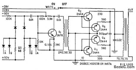
Power amplifier is followed by impedance-changing device that converts voltage waveform at output of flip-flop into corresponding cur rent waveform for low-impedance recording head of magnetic memory drum, for Manchester recording with 220 ma peak-to-peak.-A. J. Strassman and R. E. Keeter, Clock Track Recorder For Memory Drum, Electronics, 32:41, p 74-76. (View)
View full Circuit Diagram | Comments | Reading(1271)
BANDPASS_AMPLIFIER_DRIVES_RECORDER
Published:2009/7/20 1:08:00 Author:Jessie
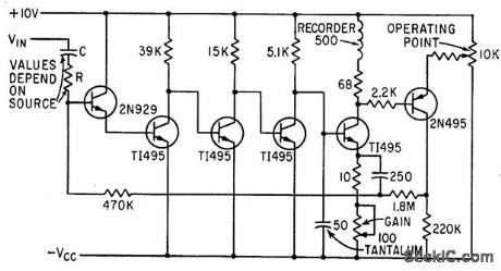
Feedback from final stage to input sets bias level of direct-coupled ac amplifier having current-derived stabilization, for driving re carder over range of 0.2 to 5 cps, with no bulky capacitors.-P. Laakmann, Direct Coupling Shrinks Amplifier Size and Cost, Electronics, 36:12, p 66-68. (View)
View full Circuit Diagram | Comments | Reading(1220)
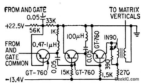
SHOCKPROOF_FERRITE_CORE_RECORDER
Published:2009/7/20 1:05:00 Author:Jessie
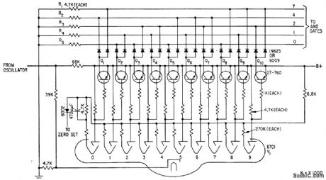
Cores retain stored data even alter 6,000-9 shock. Each transistor encodes decimal digit into two binary digits. Beam-switching decade counter makes Q1 to Q10 count in succession, to energize the lye outputs that pulse cores through gated amplifiers.-C. P. Hedges, Digital Recorder Holds Data After Shock, Electronics, 32:12, p 60--62. (View)
View full Circuit Diagram | Comments | Reading(1030)
AUDIO_GENERATOR
Published:2009/7/10 1:35:00 Author:May
This circuit produces a sinusoidal output of about 8 V pk-pk, which can be varied down to zero, at about 500 Hz. The signal is generated by a phase-shift oscillator. (View)
View full Circuit Diagram | Comments | Reading(1525)
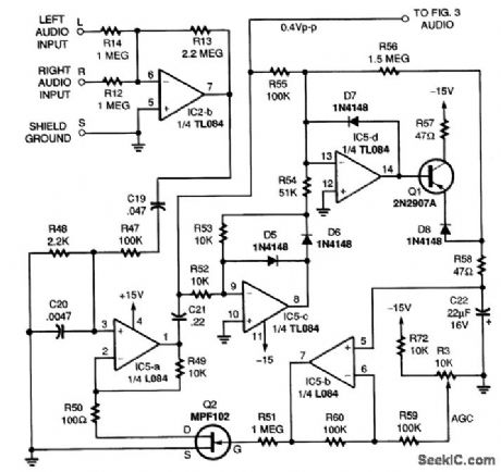
AUDIO_COMPRESSOR_AUDIO_BAND_SPLITTER
Published:2009/7/9 22:31:00 Author:May
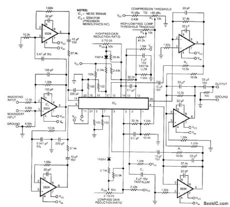
This 2-band compressor splits the audio into high and low frequencies and allows independent adjustment of each. Two active filters drive the two halves of dual voltage controlled amplifier/rectifter IC. Each section has a dynamic range greater than 100 dB. Compression gain slopes are adjustable from 2 to 25 for both audio bands. RB adjusts the threshold amplitude between the two bands. RK1 and R2/C2 control the compressor attack times (10 kΩ and 2 μF, respectively), while the 1.5-MΩ) resistor in the integrator circuit controls the release line. (View)
View full Circuit Diagram | Comments | Reading(2928)
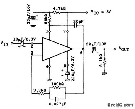
VSUBCC_SUB__AUDIO_NOISE_REDUCER
Published:2009/7/20 3:12:00 Author:Jessie
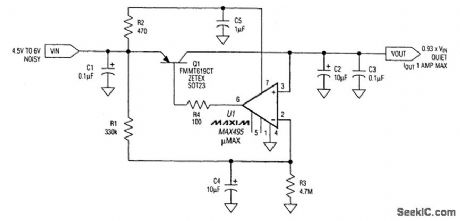
The circuit reduces noise and ripple voltage by 40 dB over the 100-Hz to 20-kHz audio range. It provides a clean source of 5-V power for driving audio circuits in portable applications such as cellular phones and multimedia notebook computers. Most linear regulators reject noise only up to 1000 Hz or so, and the bulk of a low-frequency passive filter is unwelcome in portable applications. The circuit shown accepts noisy Vcc in the 4.5- to 6-V range and produces quiet Vcc at a dc level 7 percent lower. For example, it produces 4.65 V at 1 A from a nominal 5-V source, with only 200 μA of quiescent current. The largest capacitor is 10 μF and the resistors can be 0.1 W or surface-mount 0805 size. When operating, the circuit acts as a wide-bandwidth buffered voltage follower (not a regulator) whose dc output level is 7 percent below Vin。 R1 and R3 form a voltage divider that provides the 7 percent attenuation, and C4 helps to form a 93-percent filter replica of Vin at the op amp's inverting input. The op amp's small input bias current (25 nA typical) allows large resistor values for R1 and R3, yet limits the maximum dc error to only 20 mV. The result is a low-pass filter with a 2-Hz corner frequency that provides 20 dB of attenuation at 20 Hz. (View)
View full Circuit Diagram | Comments | Reading(1253)
PERIODIC_60_Hz_NOISE_ELIMINATOR
Published:2009/7/20 3:05:00 Author:Jessie
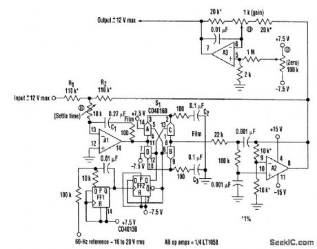


This analog/digital synchronous-averager circuit implements a robust comb filter that (theoretically) infinitely attenuates all 60-Hz harmonics. It does this independently of precision component tolerances. Signal components with frequencies below 20 Hz are passed virtually undisturbed. In the circuit, A1 continuously integrates and inverts the sum of the input signal and the output of buffer amplifier A2. Depending on the state of FF2, either switches S1A and S1B or S1C and S1D will conduct. Because flip-flop FF2 toggles once each 60-Hz cycle, A1 always integrates the difference between the instantaneous input voltage and the integral of the input taken over the preceding cycle. The transfer function of such a piecewise integration is characterized by a series of impulses that occurs atƒ (the fundamental frequency of the integration cycle) and at all integer multiples ofƒ This extreme attenuation of harmonic noise is not limited by component tolerance. The filter's setting time for an input step, however, does depend upon the trimming of potentiometer P1. Optional unity-gain inverter A3 undoes the signal inversion performed by A1 and incorporates trimmer pots P2 and P3 for precise adjustment of overall filter gain and zero offset. (View)
View full Circuit Diagram | Comments | Reading(1729)
MUSIC_VISION_CIRCUIT
Published:2009/7/20 3:00:00 Author:Jessie
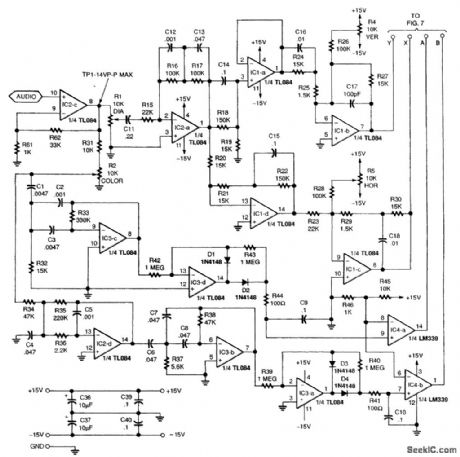
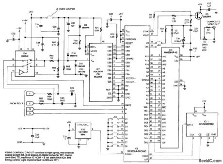
The basic concept involves processing an audio signal input into two components (x and y) that are phase-shifted approximately 90° relative to each other. The signals are then digitally sampled and stored in a video RAM buffer as an array of data bits. Bit locations in RAM correspond with the horizontal(x value) and vertical (y value) positions of points to be illuminated on the TV screen. The video RAM is periodically read and erased in synchronism with video frame scanning. The resulting serial video data is combined with color burst and sync signals to generate an NTSC-compatible composite video output signal. The music vision circuit essentially converts the standard raster-scanned TV screen into an oscilloscope-type display in which horizontal and vertical positions are directly controlled by z and y signals. The 90° phase shift between the two signals generates complex and dynamic two-dimensional patterns on the TV screen when music, voice, or other audio signals are applied to the input. The audio-frequency content of the input signal determines the color of the video pattern being displayed. (View)
View full Circuit Diagram | Comments | Reading(2289)
ANALOG_DELAY_FLANGING_UNIT_
Published:2009/7/20 2:48:00 Author:Jessie
Audio from the guitar is fed first to a preamp and LP filter, then through an analog delay line IC. The delay is a function of clock frequency. The clock frequency, and, therefore, the delay time of the line, can be modulated by a low-frequency oscillator. This gives the characteristic sound to the guitar audio. (View)
View full Circuit Diagram | Comments | Reading(2225)
NAB_98_cm_s_equalizer_amplifier_for_car_stereo_using_an_ECG1087_module
Published:2009/7/20 4:03:00 Author:Jessie
NAB 9.8 cm/s equalizer amplifier for car stereo using an ECG1087 module. Typical voltage gain is 35 dB (courtesy GTE Sylvania Incorporated). (View)
View full Circuit Diagram | Comments | Reading(1139)
General_purpose_voltage_preamplifier
Published:2009/7/20 4:42:00 Author:Jessie
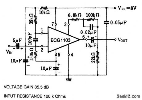
General-purpose voltage preamplifier. Typical voltage gain is 35.5 dB. Input resistance is 120K. The EGG1103 is a 7-pin module (courtesy GTF Sylvania). (View)
View full Circuit Diagram | Comments | Reading(972)
SIMPLE_UTILITY_MIXER
Published:2009/7/9 5:07:00 Author:May
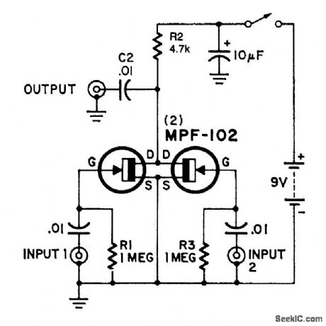

Here's an interesting mixer circuit. With it you can effectively combine signals from audio to high-fre-quency RF. Also, as a special bonus, this circuit will provide some gain at a low noise figure. The inputs can be of almost any level or impedance, and the output (low-Z) will drive most tuned circuits or transistors.Basically, the device consists of two similar FET amplifier stages with a common load resistor (R2). Each FET develops a signal across this resistor, a form of cancellation occurs, and a difference signal results.If you want less gain, try reducing R2 to 2200-Ω. This modification will not affect the mixing ability.
(View)
View full Circuit Diagram | Comments | Reading(2168)
AUDIO_MIXER
Published:2009/7/9 4:58:00 Author:May
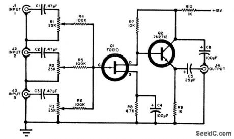
Three audio circuits are combined in the circuit shown. Each input is coupled to its own level potenti-ometer (R1, R2, or R3) and they are combined at the gate of FET Q1. The output of Q1 is coupled to the external audio amplifier through emitter-follower Q2 and capacitor CG. (View)
View full Circuit Diagram | Comments | Reading(0)
45_watt_AF_power_amplifier_for_a_4_ohm_load
Published:2009/7/20 5:31:00 Author:Jessie
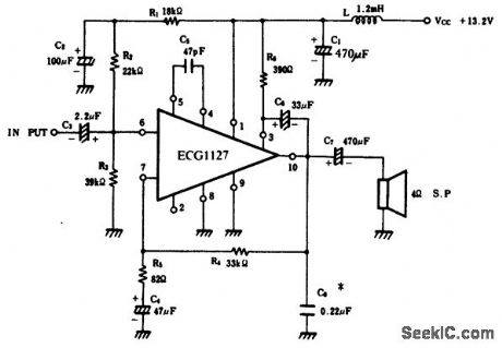
4.5-watt AF power amplifier for a 4-ohm load. Recommended supply voltage is 13.2 volts, which makes this circuit ideal for automotive applications. Typical voltage gain is 50 dB (courtesy GTE Sylvania Incorporated). (View)
View full Circuit Diagram | Comments | Reading(915)
4_watt_OTL_power_amplifier_using_10_pin_TO3
Published:2009/7/20 5:30:00 Author:Jessie
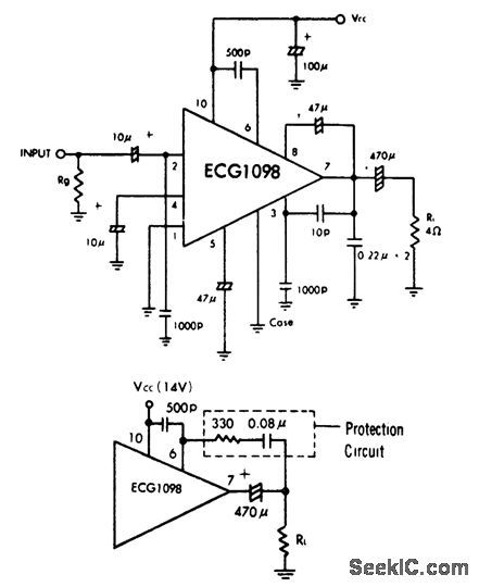
4-watt OTL power amplifier using 10-pin TO3. Typical supply voltage is 14 volts. The circuit is designed for a 4-ohm load and its efficiency is 60%. Typical voltage gain is 39 dB. Input impedance is 6.5K. Bandwidth is 70 hertz to 20 kilohertz. Although the ECG1098 can handle short-circuit conditions for short durations, it is recommended that the protection circuit shown be used if long periods with the speaker load shorted occur (courtesy GTE Sylvania Incorporated). (View)
View full Circuit Diagram | Comments | Reading(1008)
4_INPUT_UNITY_GAIN_MIXER
Published:2009/7/9 4:45:00 Author:May
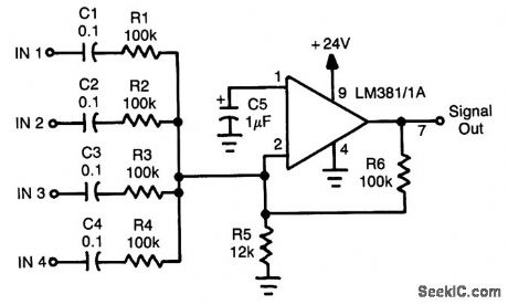
An LM381/1Ais used as a four-input unity-gain audio mlxer. Gain can be increased decreasing R1 through R4 or increasing R6. (View)
View full Circuit Diagram | Comments | Reading(3169)
DIGITAL_MIXER
Published:2009/7/9 4:40:00 Author:May
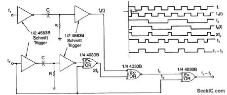
A simple digital mixer, based on two dual-Schmitt triggers (4583B) and three exclusive-OR gates, uses an RC time-delay circuit to permit easy adjustment of the output-signal pulse width. The exclusive-OR gates ,can also be used separately as a symmetrical frequency doublet.As shown, a signal passing through the Schmitt triggers is delayed by t, a value equal to RC In (VTP/VTN)where Vtp and Vtn are the positive and negative threshold voltages of the triggers.To function properly, the same time delay must be introduced to signals f1 and f2. Also, the time delay must be less than 50%of the period of f1. Provided that f1 is more than twice the value of f2, the output of the circuit will equal the difference of the two signals (i.e., f1 - f2). (View)
View full Circuit Diagram | Comments | Reading(2584)
10_watt_UHF_microstrip_amplifier_for_450_to_470_MHz
Published:2009/7/20 7:31:00 Author:Jessie
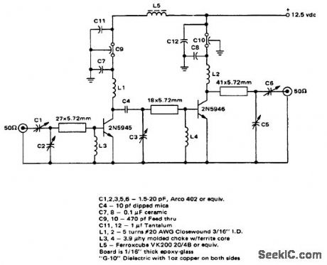
10-watt UHF microstrip amplifier for 450 to 470 MHz (courtesy Motorola Semiconductor Products Inc.). (View)
View full Circuit Diagram | Comments | Reading(1162)
| Pages:19/54 1234567891011121314151617181920Under 20 |
Circuit Categories
power supply circuit
Amplifier Circuit
Basic Circuit
LED and Light Circuit
Sensor Circuit
Signal Processing
Electrical Equipment Circuit
Control Circuit
Remote Control Circuit
A/D-D/A Converter Circuit
Audio Circuit
Measuring and Test Circuit
Communication Circuit
Computer-Related Circuit
555 Circuit
Automotive Circuit
Repairing Circuit