
Audio Circuit
Index 3
Practical tones preamp circuit diagram
Published:2014/1/16 21:52:00 Author: | Keyword: Practical tones preamp circuit diagram, LM1036
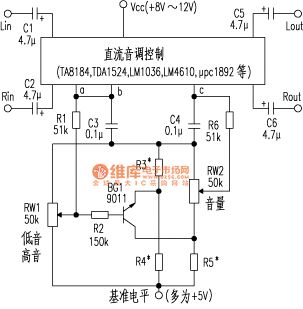
The core parts of the circuit by a dc tone control IC, a NPN transistor, and four resistors common enough. Other components are used in the dc tone control IC itself needs to peripheral components. Most dc tone control IC has himself to dc tone control circuit provides a reference level (mostly + 5 v), but mu PC1892 dc tone control IC, such as exception, must by external with + 5 v dc reference level. Figure 1 for this function circuit schematic diagram, figure 2 as an example.
Component parameter setting: as high and low adjusting potentiometer RW1 is in not ascend, BG1 should be ended, no influence of volume at this time. As high and low adjusting potentiometer RW1 from start to ascend, and finally achieve maximum lifting capacity + 12 db, BG1 by the globe into linear workspace, and then further into conducting state completely, leading to add on the volume potentiometer dc level to reduce the dc tone control IC output signal amplitude attenuation 12 db accordingly. Therefore, the circuit of R3, R4, R5 three selected tones of dc resistance and the associated control IC internal parameters. For example chooses dc tone control IC for the NS company LM1036 or LM1046 model, its resistance respectively choose = 22 k Ω R3 and R4 Ω Ω, R5 = 36 k = 5.6 k.
As shown practical tones preamp circuit diagram
(View)
View full Circuit Diagram | Comments | Reading(1554)
Audio amplifier circuit diagram
Published:2014/1/16 18:35:00 Author: | Keyword: Audio amplifier circuit diagram,
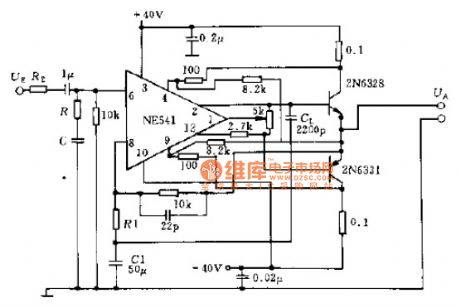
Diagram using NE541 high voltage power amplifier, current gain in 20 ~ HZ20KHZ frequency range is 90 db, at 300 mv RMS input, output high level RMS 20 v. integrated circuit internal equipped with short circuit protection. The external current limiting network to provide additional protection, two output transistor to increase the output power to 75 w, to drive the speakers.
Audio amplifier circuit diagram as shown
(View)
View full Circuit Diagram | Comments | Reading(1406)
D2025 dual channel audio amplifier circuit diagram
Published:2014/1/14 18:21:00 Author: | Keyword: D2025 dual channel audio amplifier circuit diagram, D2025, DIP16
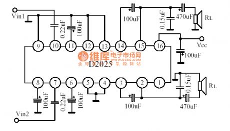
D2025 dual-channel audio power amplifier circuit D2025 stereo audio power amplifier integrated circuits for power amplifier using DIP16 package applicable to all types of portable tape recorders or portable stereo. Suitable for dual symmetrical or BTL wide-range supply voltage connections (3V ~ 12V) Maximum voltage gain 45dB (can be adjusted by an external resistor 3V low pressure under normal use.
As shown D2025 dual-channel audio amplifier circuit diagram
(View)
View full Circuit Diagram | Comments | Reading(5461)
D2003 power amplifier circuit diagram
Published:2014/1/13 22:17:00 Author: | Keyword: D2003 power amplifier circuit diagram,
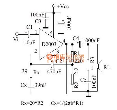
D2003 power amplifier circuit diagram as shown (View)
View full Circuit Diagram | Comments | Reading(1323)
Typical application circuit diagram TDA2616 audio power amplifier circuit
Published:2014/1/13 18:35:00 Author: | Keyword: Typical application circuit diagram TDA2616 audio power amplifier circuit, TDA2616
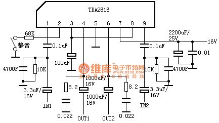
TDA2616 pin functions and reference voltage:
1 Foot: 10V - Signal Input 1
2 Feet: 5V - Squelch (low squelch)
3 Feet: 10V - 1/2 reference voltage
4 Feet: 10V - Signal output 1
5 feet: 0V - ground
6 Feet: 10V - Signal output 2
7 Feet: 20V - Power
8 feet: 10V - negative inputs
9 feet: 10V - Signal Input 2
Application Notes TDA2616 audio amplifier circuit shown in Figure typical
(View)
View full Circuit Diagram | Comments | Reading(11160)
NE5532 ore radio amplifier circuit diagram
Published:2014/1/13 18:30:00 Author: | Keyword: NE5532 ore radio amplifier circuit diagram, NE5532
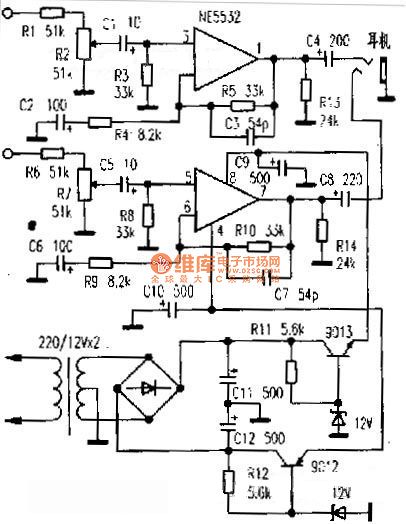
NE5532 ore radio amplifier circuit diagram as shown (View)
View full Circuit Diagram | Comments | Reading(2107)
Human body reaction velocity tester circuit diagram
Published:2014/1/13 0:59:00 Author: | Keyword: Human body reaction velocity tester circuit diagram,
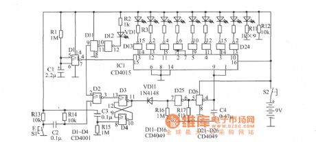
Human body reaction velocity tester circuit diagram
The human body reaction speed tester circuit as shown. Nand gate D25, D26 multivibrator, the output clock pulse cycle of about 50 ms. IC1 composed of eight moves to the right register, boot of D1 delay circuit output signal as a serial input data. Just when switched on, because of the D1 output is 1 , under the effect of clock pulse, the IC1 8-bit register unit quickly for all 1 ; After 3 ~ 4 s s, D1 output into a 0 , the test lamp VD1 bright, at the same time, the IC1 8-bit register units will be under the effect of clock pulse from left to right in turn into a 0 , until they are testing people press the stop button S1, D3, D4 RS flip-flop consisting of 0 , make the D25, D26 stop, keep IC1, the result through the drive circuit D13 ~ D16, D21 ~ D24 drive led display. D2 role is to make the stop button S1 only after the test signal VD1 light works, press ahead is invalid. (View)
View full Circuit Diagram | Comments | Reading(1315)
Typical application circuit diagram TDA2009 audio power amplifier circuit
Published:2014/1/13 0:55:00 Author: | Keyword: Typical application circuit diagram TDA2009 audio power amplifier circuit, TDA2009
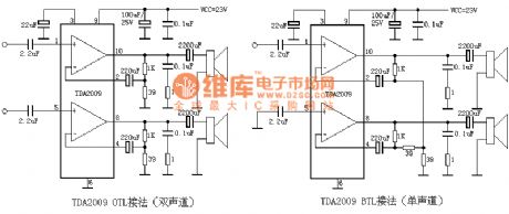
TDA2009
1-Foot: 1.2V-- Left channel input
2-Feet: 0.8V-- Left channel feedback
3 Feet: 12V - Squelch
4-Feet: 0.8V-- right channel feedback
5 Feet: 1.2V-- right channel input
6 Feet: 0V - ground
7 Feet: 0V - empty
8 feet: 12.4V-- right channel output
9 feet: 24V - Power
10 feet: 12.4V-- Left channel output
Application Notes TDA2009 audio amplifier circuit shown in Figure typical
(View)
View full Circuit Diagram | Comments | Reading(1968)
Typical application circuit diagram TDA1521 audio power amplifier circuit
Published:2014/1/13 0:38:00 Author: | Keyword: Typical application circuit diagram TDA1521 audio power amplifier circuit, TDA1521
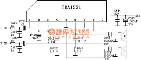
The circuit is taken from Changhong C2191, dual-channel access method for the OTL.
TDA1521 pin functions and reference voltage:
1 foot: 11V - Reverse Input 1 (L-channel signal input)
2 feet: 11V - Forward Input 13 feet: 11V - Reference 1 (when OCL connection to 0V, when OTL connection to 1/2Vcc)
4 feet: 11V - Output 1 (L-channel signal output)
5 feet: 0V - Negative power input (OTL connection when ground)
6 Foot: 11V - Output 2 (R channel signal output)
7 Foot: 22V - Positive power supply input
8 feet: 11V - positive input 2
9 feet: 11V - Reverse Input 2 (R-channel signal input)
Application Notes TDA1521 audio amplifier circuit shown in Figure typical
(View)
View full Circuit Diagram | Comments | Reading(3843)
Typical application circuit diagram TA8211AH audio power amplifier circuit
Published:2014/1/13 0:30:00 Author: | Keyword: Typical application circuit diagram TA8211AH audio power amplifier circuit, TA8211AH
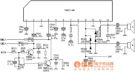
The circuit is taken from Changhong C2588-shaped TV
Pin 1: 2.1V-- Left channel negative feedback external capacitor
Pin 2: 2.2V-- left channel signal input
Pin 3: 0V - ground
Pin 4: 2.2V-- right channel signal input
Pin 5: 2.1V-- Right channel negative feedback external capacitor
Pin 6: 8.2V-- Power Filter
Pin 7: 12V - right channel signal output
Pin 8: 2.2V-- empty
Pin 9: 24V - Power
Pin 10: 2.2V-- empty
Pin 11: 12V - left channel signal output
Diagram TA8211AH typical audio amplifier circuit shown in Figure
(View)
View full Circuit Diagram | Comments | Reading(4693)
Typical application circuit diagram LA4287 audio power amplifier circuit
Published:2014/1/13 0:31:00 Author: | Keyword: Typical application circuit diagram LA4287 audio power amplifier circuit, LA4287
TV audio signal from ( 1 ) pin input N601 's , AV audio signal from ( 3 ) feet of the input N601 , CPU (40) pin output TV / AV switching signal via the base of R601 to V601 , V601 inverted by the after controlling N601 's ( 4 ) feet , after an internal selection ( 9 ) pin outputs an audio signal from the N601 , pushing the horn sound.
V641, V642 audio squelch circuit consisting shutdown : normal boot , 12V voltage is applied through R641 base V641 , V641 has been added to the emitter VD642 , VD642 because of the presence of so than the base -emitter voltage V641 high voltage 0.7V, V641 deadline , V642 also cut , this circuit has no effect on the volume control , then, the C641 is near the 12V charging voltage . After the shutdown , 12V voltage disappears , since the case is filled with the C641 12V voltage , so the base voltage V641 is lower than the emitter voltage , V641 conduction , V642 is also on, the volume control voltage is shorted to ground , to achieve a static off noise .LA4287 pin functions and reference voltage:
Pin 1 : 6.3V-- Signal Input 1
Pin 2 : 0V - ground
Pin3 6.3V-- Signal Input 2
Pin 4: 2.1V-- signal switch
Pin 5: 0.67V-- Volume control voltage input
Pin 6: 9.8V-- Filter
Pin 7: 9.8V-- Feedback
Pin 8: 0V - ground
Pin 9: 9.9V-- Output
Pin 10: 21V - Power
Diagram LA4287 typical audio amplifier circuit shown in Figure
(View)
View full Circuit Diagram | Comments | Reading(1688)
Typical application circuit diagram AN5265 audio power amplifier circuit
Published:2014/1/9 20:01:00 Author: | Keyword: Typical application circuit diagram AN5265 audio power amplifier circuit, AN5265
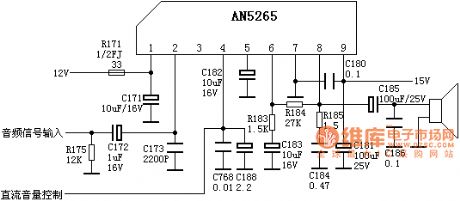
AN5265 pin functions and reference voltage:
Pin 1: 12V - Front-level power
Pin 2: 5V - audio signal input
Pin 3: 0V - Mute control terminal (high Mute)
Pin 4: 0.1V-- Volume control voltage input terminal
Pin 5: 7V - Filtering end
Pin 6: 7.4V-- Negative feedback input
Pin 7: 0V - ground
Pin 8: 7.5V-- the output of the power amplifier
Pin 9: 15V - power amplifier stage
Application Notes AN5265 typical audio amplifier circuit shown in Fig.
(View)
View full Circuit Diagram | Comments | Reading(4424)
Typical application circuit diagram LA4225A audio power amplifier circuit
Published:2014/1/9 19:58:00 Author: | Keyword: Typical application circuit diagram LA4225A audio power amplifier circuit, LA4225A
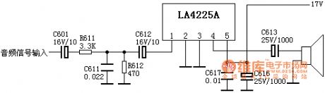
Diagram LA4225A typical audio amplifier circuit shown in Figure (View)
View full Circuit Diagram | Comments | Reading(1885)
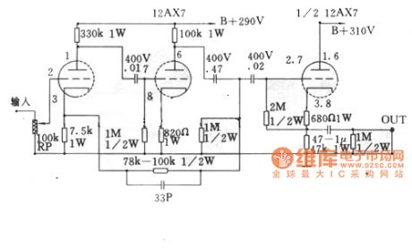
6 v6 bile machine circuit diagram
Published:2014/1/2 19:53:00 Author: | Keyword: 6 v6 bile machine circuit diagram,
Rectifier uses a buffer to protect the front 5Z4P level after level using two tubes using four 6P6P/6V6 use RiFa cathode capacitance, coupling capacitance adjustment silver foot audio tone.
6V6 tube amp circuit shown in Figure
(View)
View full Circuit Diagram | Comments | Reading(1657)
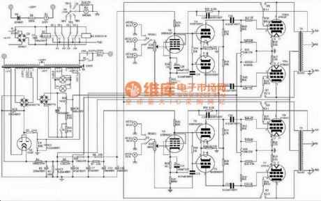
McLntosh 275 bile machine power amplifier circuit diagram
Published:2014/1/1 19:47:00 Author: | Keyword: McLntosh 275 bile machine power amplifier circuit diagram, KT88
McLntosh level 275 amplifier power amplifier tube using KT88 OR 6550 for each channel output can reach 60 watts, nonlinear distortion less than 1%, the frequency response of 20 hz ~ 30 KHZ, plus OR minus 0.5 dB.
McLntosh 275 as shown bravery machine power amplifier circuit diagram
(View)
View full Circuit Diagram | Comments | Reading(1884)
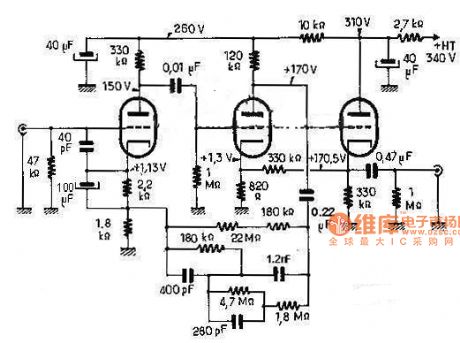
McLntosh C22 bile machine circuit diagram
Published:2014/1/1 19:43:00 Author: | Keyword: McLntosh C22 bile machine circuit diagram,
A circuit diagram as shown McLntosh C22 bile machine (View)
View full Circuit Diagram | Comments | Reading(1413)
McLntosh C22 power amplifier circuit diagram
Published:2014/1/1 19:37:00 Author: | Keyword: McLntosh C22 power amplifier circuit diagram,
As shown in figure McLntosh C22 power amplifier circuit diagram (View)
View full Circuit Diagram | Comments | Reading(1048)
Mini Metronomes
Published:2013/7/30 20:37:00 Author:muriel | Keyword: Mini Metronomes
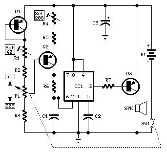
Parts:P1 100K Linear PotentiometerR1 10K 1/2W Trimmer CermetR2 10K 1/4W ResistorR3 330K 1/4W ResistorR4 50K 1/2W Trimmer CermetR5 100K 1/4W ResistorR6,R7 1K 1/4W ResistorC1 1µF 63V Polyester CapacitorC2 10nF 63V Polyester CapacitorC3 47µF 25V Electrolytic CapacitorIC1 NE555 General purpose timer ICQ1,Q2 BC560 45V 100mA Low noise High gain PNP TransistorsQ3 ZTX753 100V 2A PNP TransistorSW1 SPST Switch (Ganged with P1)SPK 8 Ohm 40mm. Loudspeaker B1 12V Battery (MN21, GP23A or VR22 type)
Notes:Q1 & Q2 provide linear frequency operation of IC1 following P1 resistance variation.Q3 was added in order to obtain a louder click, similar to clockwork metronomes.12V micro battery was used to obtain more output power and more compactness.Rotate P1 fully towards R2, then set R1 to obtain 40 beats per minute (compare with another metronome).Rotate P1 fully towards R3, then set R4 to obtain 208 beats per minute.Finally mark the entire scale with the usual metronome steps as following:40 - 42 - 44 - 46 - 48 - 50 - 52 - 54 - 58 - 60 - 63 - 66 - 69 - 72 - 76 - 80 - 84 - 88 - 92 - 96 - 100 - 104 - 108 - 112 - 116 - 120 - 126 - 132 - 138 - 144 - 152 - 160 - 168 - 176 - 184 - 192 - 200 - 208. (View)
View full Circuit Diagram | Comments | Reading(1320)
WAILING SIREN
Published:2013/7/29 1:49:00 Author:lynne | Keyword: WAILING SIREN
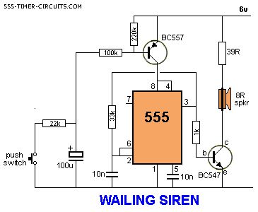
By pressing the button, the wailing sound increases. Releasing the button decreases the wailing. The circuit automatically turns off after about 30 seconds.
(View)
View full Circuit Diagram | Comments | Reading(0)
Nostalgic Crystal Radio
Published:2013/7/21 20:22:00 Author:muriel | Keyword: Nostalgic Crystal Radio
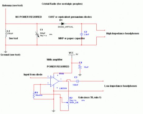
It was the first circuit i started with, and it can be build with really junk items. Apart from the diode (which replacement would need a PbS, Lead Sulphyde, galena cristal) everything you can see in the circuit (for the no power version) can be built with enamel wire, alluminium cooking foil, carton wax and so on. The real painful part is to find a high impedance headphone, it is unlikely yo find one at present day but it is possible. In addition I substituted an high internal impedance headphone with a opamp and normalheadphone but doing so you need power. Anyway if you are lucky you can find such a headphone.
Operating Principle:The AM signal is captured by the antenna , 10 mt long horizontal wire, WELL insulated from earth (I mean distant, to lower the stray capacitance coupling with ground which will adsorb some signal ). The Inductor and capacitor forms a resonator, that will tune with the station which frequency is F= 1/ (2*pi*sqrt(L*C)), so adjust C1 for tuning. The signal is rectified (demodulated) and smoothed by C2. The high impedance headphones has fine internal wiring and lots of windings, so even a small current will produce an audio output.
Construction of components:
Antenna:10 mt of electrical wire, WELL insulated from ground (use plastic bottle caps and hoowup wire to keep it high). This must be the arrangement |=wall ..=hookup wire o=plastic cap --=wire antenna :| 10 mt |wall |...O...O...O----------------------------------O...O...O...| wall| | |to receiver
Inductor:wind 60 windings of enamel copper wire onto a 2 inch ferrite core (1 cm diameter or a bit less)
RF GROUND:Like for tesla coils, it must be a good ground, otherwire the signal will be poor. Place a metal nail and connect to the circuit with alligator clips.
C1:It would be difficult to make it reliable, in addition needs a capacitance meter, better buing it or finding it in old broken radios.But if you want to build it use the parallel plate capacitance formula and make two carton disks (10 cm diameter with a alu foil semi disk each separated through paper, place a nail in center (make sure to not short the capacitor) and connect it with small wires, rotating a disk respect to the other will change shared surface and increase capacitance, but how i said this is not reliable because as soon ase you approach it, you will detune it. So better use a commercial variable cap with insulated lever.
C2:use paper, alu foil or ldpe (but i don't think that you will be interested in a 10KV capacitor so use thin LDPE)
Diode:Buy it. I don't advice you looking for Lead Sulphyde cristals....
High impedance headphones: Difficult to find , the only substitute is an amplifier (see below)
Amplifier + low impedance headphones: Use a general purpose opamp with feedback resistors and a low impedance headphone (as these of cassette, cd players), but you need power... :-(
It is very nice to build, hearing a sound of a radio station without power is very fun. I reconstrected it basing on my fathers rememberings and very old texts, improved a bit with some physics. Constructing from almost anything is possible , even the headphone, as many cristal radios have been found in nazis prison camps build by prisoners from very limited resources (as everything in a prison camp) and some in foxholes (called foxhole radios).
Anyway, as i ever say, learn and have fun (View)
View full Circuit Diagram | Comments | Reading(1315)
| Pages:3/54 1234567891011121314151617181920Under 20 |
Circuit Categories
power supply circuit
Amplifier Circuit
Basic Circuit
LED and Light Circuit
Sensor Circuit
Signal Processing
Electrical Equipment Circuit
Control Circuit
Remote Control Circuit
A/D-D/A Converter Circuit
Audio Circuit
Measuring and Test Circuit
Communication Circuit
Computer-Related Circuit
555 Circuit
Automotive Circuit
Repairing Circuit