
Automotive Circuit
Index 18
The muscle stretch tester circuit
Published:2011/8/23 22:14:00 Author:Borg | Keyword: muscle stretch tester
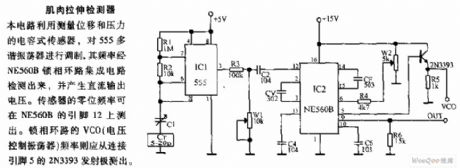
The circuit modulates 555 multi-resonance by using the capacitance sensor that measures movement and pressure, the frequency is tested out by the NE560B PLL integrated circuit, and it generates the DC output voltage. The sensor zero frequency can be tested out by the 12-pin of NE560B. The VCO (voltage control oscillator) frequency of the PLL circuit should be tested out from the 2N3393 emitter which connects with 5-pin.
(View)
View full Circuit Diagram | Comments | Reading(793)
The amplifier pin and main features--the XR4202 4-line calculator and silent low-power op-amp
Published:2011/8/25 4:03:00 Author:Borg | Keyword: amplifier pin, calculator, op-amp
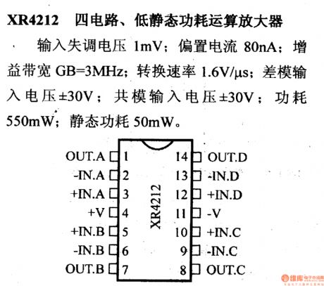
the XR4202 4-line calculator and silent low-power op-ampThe input offset voltage is 1mV; the biased current is 80nA; the gain band width GB=3.5MHz; the converting ratio is 1.6V/μs; the differential mode input voltage is ±30V; the common mode input voltage is ±30V; the power consumption is 550mW; the static power consumption 50mW.
(View)
View full Circuit Diagram | Comments | Reading(740)
The amplifier pin and main features--XR4202 programmable 4-line calculator
Published:2011/8/25 3:57:00 Author:Borg | Keyword: amplifier pin, calculator
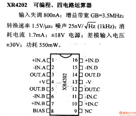
XR4202 programmable 4-line calculatorThe input offset voltage is 2mV; the gain band width is GB=3.5MHz; the converting ratio is 1.5V/μs; the noise is 25nV/(1KHz); the consumption current is 1.7mA; the power supply voltage is ±18V; the differential mode input voltage is ±30V; the power consumption is 550mW.
(View)
View full Circuit Diagram | Comments | Reading(725)
The amplifier pin and main features--the TL322 op-amp of dual-single power supply
Published:2011/8/25 3:51:00 Author:Borg | Keyword: amplifier pin, op-amp, dual-single power supply
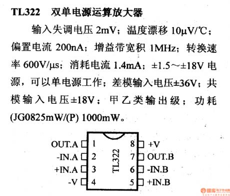
The TL322 op-amp of dual-single power supply The input offset voltage is 2mV; the temperature drift is 10μV/℃; the biased current is 200nA; the gain band width is 1MHz; the converting ratio is 600V/μs; the consumed current is 1.4mA; the voltage of the power supply is ±1.5~±18V, it can work with a single power supply; the differential mode input voltage is ±36V; the common mode input voltage is ±18V; its output stage is divided into 2 types which are A and B; its power consumption is (JG0825mW/(P)1000mW).
(View)
View full Circuit Diagram | Comments | Reading(749)
The amplifier pin and main features--the TL321 op-amp of single power
Published:2011/8/25 3:39:00 Author:Borg | Keyword: amplifier pin, op-amp
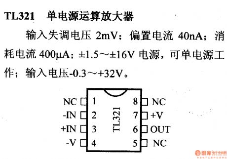
TL321--the single power supply op-ampThe input offset voltage is 2mV; the biased current is 40nA; the consuming current is 400μA; the voltage of the power supply is ±1.5~±16V, it can work with a single power supply; the input voltage is -0.3~+32V.
(View)
View full Circuit Diagram | Comments | Reading(1025)
The amplifier pin and main features--the general JEFT input op-amp of TL081
Published:2011/8/25 1:04:00 Author:Borg | Keyword: amplifier pin, general JEFT, input op-amp
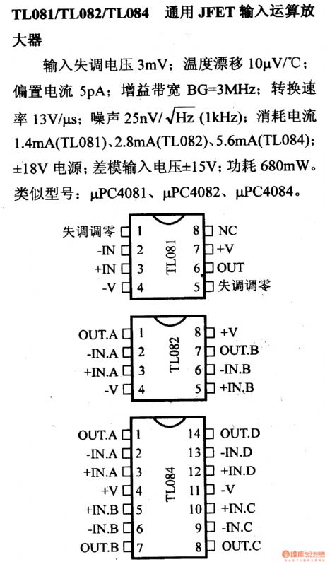
TL081/TL082/TL084--the general JFET input op-ampThe input offset voltage is 3mV; the temperature drift is 10μV/℃; the input bias current is 5pA; the gain band width is GB=3MHz; the converting speed rate is 13V/μs; the noise is 25nV/(1KHz); the consumed current is 1.4mA/(TL081), 2.8mA(TL082), 5.6mA(TL084); the power supply is ±18V; the differential mode input voltage is ±15V; the power consumption is 680mW. The approximate types are μPC4081, μPC4082 and μPC4084.
(View)
View full Circuit Diagram | Comments | Reading(2419)
The amplifier pin and main features--the TL136 op-amp of 4 high functions
Published:2011/8/25 1:16:00 Author:Borg | Keyword: amplifier pin, op-amp
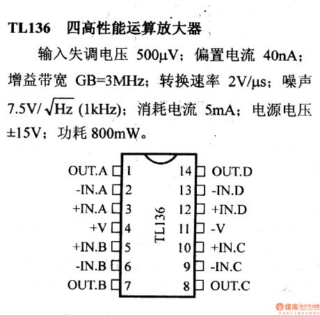
TL136--the TL136 op-amp of 4 high functionsThe input offset voltage is 500μV; the biased current is 40nA; the gain band width is GB=3MHz; the converting speed rate is 2V/μs; the noise is 7.5nV/(1KHz); the consumed current is 5mA; the power supply voltage is ±15V; the power consumption is 800mW.
(View)
View full Circuit Diagram | Comments | Reading(729)
The amplifier pin and main features--the single power supply JEFT input op-amp of TL091
Published:2011/8/25 1:11:00 Author:Borg | Keyword: amplifier pin, general JEFT, input op-amp
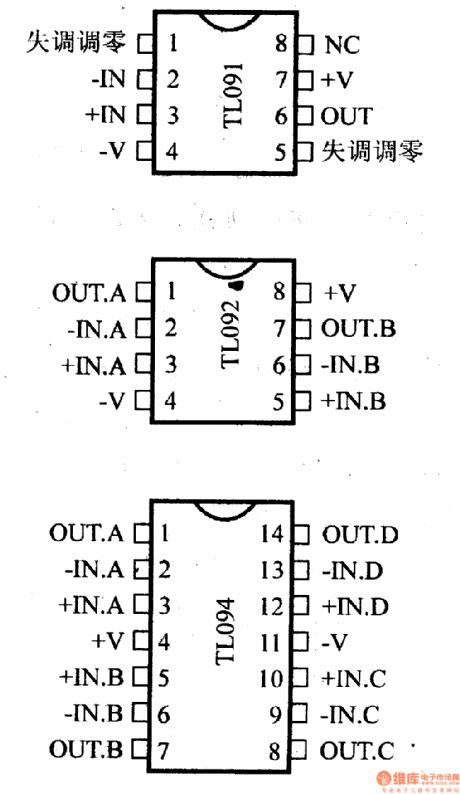
TL091/TL092/TL094--the single power supply JEFT input op-ampThe input offset voltage is 5mV; the temperature drift is 10μV/℃; the input bias current is 200pA; the gain band width is GB=1MHz; the converting speed rate is 600mV/μs; the noise is 34nV/(1KHz); the consumed current is 1.5mA/(TL081), 3mA(TL082), 6mA(TL084); the power supply is ±1.5~±18V; it can work with a single power supply; the differential mode input voltage is ±36V; the common mode input voltage is ±18V; the power consumptions are (J)1025mW and (N)1150mW.
(View)
View full Circuit Diagram | Comments | Reading(1708)
The amplifier pin and main features--the general JEFT input op-amp of TL080/A
Published:2011/8/25 0:57:00 Author:Borg | Keyword: amplifier pin, JEFT, input op-amp
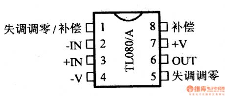
TL080/A--the general JEFT input op-ampThe input offset voltage is 3mV; the temperature drift is 10μV/℃; the input bias current is 5pA; the gain band width is GB=3MHz; the converting speed rate is 13V/μs; the noise is 25nV/(1KHz); the consumed current is 1.4mA; the power supply is ±18V; the differential mode input voltage is ±30V; the common mode input voltage is ±15V; the power consumption is 680mW.
(View)
View full Circuit Diagram | Comments | Reading(832)
The amplifier pin and main features--JEFT input op-amp of TL071
Published:2011/8/25 0:58:00 Author:Borg | Keyword: amplifier pin, op-amp, JEFT
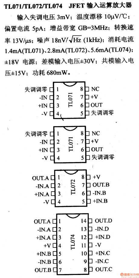
TL071/TL072/TL074--the JFET input op-ampThe input offset voltage is 3mV; the temperature drift is 10μV/℃; the biased current is 5pA; the gain band width is GB=3MHz; the converting speed rate is 13V/μs; the noise is 18nV/(1KHz); the consumed current is 1.4mA/(TL071), 2.8mA(TL072), 5.6mA(TL074); the power supply is ±18V; the differential mode input voltage is ±30V; the common mode input voltage is ±15V; the power consumption is 680mW.
(View)
View full Circuit Diagram | Comments | Reading(2716)
The main features of the amplifier pin signal--TL066/A/B programmable JFET input op-amp
Published:2011/8/23 22:14:00 Author:Borg | Keyword: amplifier, programmable JFET, input op-amp
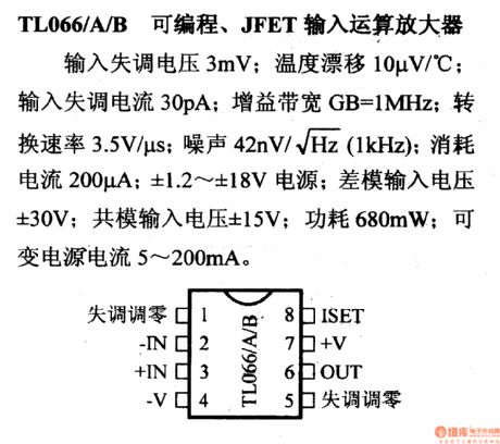
TL066/A/BprogrammableJFETinputop-amp
Input distortion voltage is 3mV; temperature drift is 10μV/⁰C; input distortion current is 30pA; gain band width is GB=1MHz; converting speed rate is 3.5V/μs; the noise 42nV/√Hz(1kHz); the current consumption is 200μA; ±1.2~±18V power supply; the differential mode input voltage is ±30V; the common mode input voltage ±15V; the power consumption is 680mW; the current of the changeable power supply is 5~200mA.
(View)
View full Circuit Diagram | Comments | Reading(983)
The main features of the amplifier pin--OPA633 buffering amplifier
Published:2011/8/23 22:14:00 Author:Borg | Keyword: amplifier pin, buffering amplifier
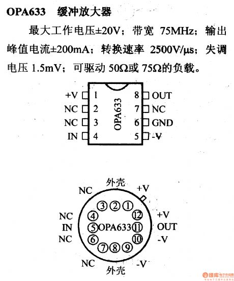
OPA633 buffering amplifier The maximum working voltage is ±20V; band width is 75MHz; output peak current is ±200mA; switching efficiency is 2500V/μS; the distortion voltage is 1.5mA; it can drive the load of 50Ω or 75Ω.
(View)
View full Circuit Diagram | Comments | Reading(861)
The visible laser Nc modulation drive
Published:2011/8/13 2:27:00 Author:qqtang | Keyword: visible, laser Nc, modulation drive
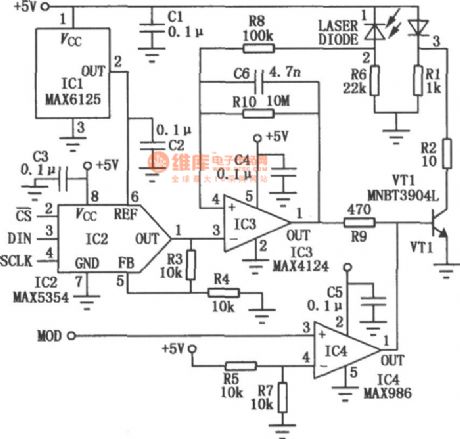
View full Circuit Diagram | Comments | Reading(630)
The capacitance phase-distribution single-phase motor connection circuit and phasor diagram
Published:2011/8/23 22:38:00 Author:qqtang | Keyword: phase-distribution, single-phase motor, connection circuit
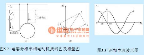
To generate a rotating field, the phase is distributed by using the serial capacitor in the starting coil, the wiring principle is shown in Figure 5.2(a). As long as the proper parameters are chosen, the phase difference between the working coil and starting coil is 90°, see as figure 5.2(b), the phase-distributed wave shape is shown in figure 5.3.
(View)
View full Circuit Diagram | Comments | Reading(1104)
The motor protector circuit
Published:2011/8/23 22:38:00 Author:qqtang | Keyword: motor protector
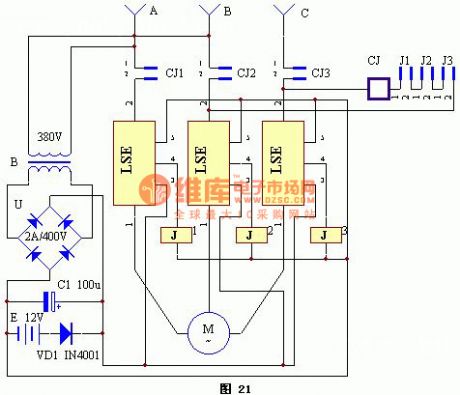
The working principle of the device is shown in figure 21. LSE component is stringed in A, B and C. When the 3-phase wire is intact, 4-pin of LSE is outputting a high LEV, meanwhile the relays of J1, J2 and J3 are in the closed state, so the 3-phase AC contcator CJ is pulled in, and the contactors of CJ1, CJ2 and CJ3 are self-protecting, the motor is working normally. If one of A, B, C 3-phase power supplies is broken down, then the part between 1-pin and 2-pin of one of the LSEs will be broken down. (View)
View full Circuit Diagram | Comments | Reading(673)
The motor phase loss protector circuit
Published:2011/8/23 22:38:00 Author:qqtang | Keyword: motor, phase loss, protector
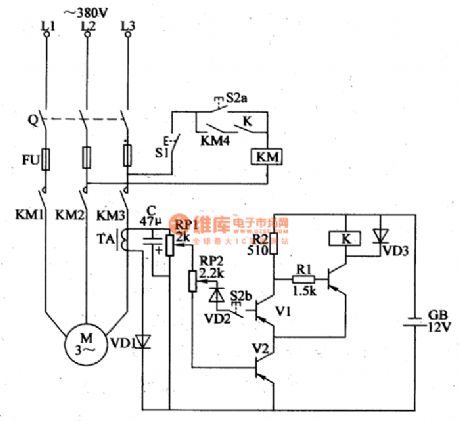
Here is to introduce a motor phase loss protector circuit, which characterizes simple circuit, low cost, easy production, stable and reliable working, no debugging and so on, it is suitable for phase loss over-current protection of intermediate and micro 3-phase motors. The working principles The motor phase loss protector consists of the current inter-inductor TAl-TA3, heat relay KR, rectifier diode VD1-VD14, relay K1-K3, starting key S1, stop key S2 and AC contactor KM,etc, see as figure 4-120.
(View)
View full Circuit Diagram | Comments | Reading(1690)
The 3-phase asynchronous motor connection circuit
Published:2011/8/23 22:38:00 Author:qqtang | Keyword: 3-phase, asynchronous motor
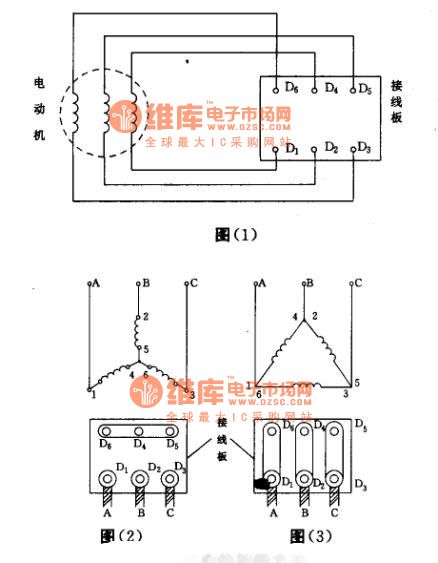
The 3-phase asynchronous motor connection circuit: each of the 3 three stator coils of the motor has 2 outgoing lines. One of them is called the head end, the other is the tail end. The head end is regulated to be represented by D1, the tail end is represented with D4; the second coil head end is represented with D2, the tail end is represented with D5; the head and tail ends of the third coil are represented with D3 and D6 respectively. The 6 outgoing lines are connected with the terminals of the box, and there are the marks of D1~D6 on the wiring terminals.
(View)
View full Circuit Diagram | Comments | Reading(2002)
The draft fan circuit (2)
Published:2011/8/23 22:38:00 Author:qqtang | Keyword: draft fan

The circuit makes sure that there is enough time when Y-△ decompression is started, i.e in the KM2 coil control circuit, the 2 couples of serial contactors make sure there is enough time when Y-△ decompression is started. (View)
View full Circuit Diagram | Comments | Reading(599)
The PVDF heart sounds impulse measuring circuit
Published:2011/8/14 22:19:00 Author:qqtang | Keyword: PVDF, heart sounds, impulse measuring circuit
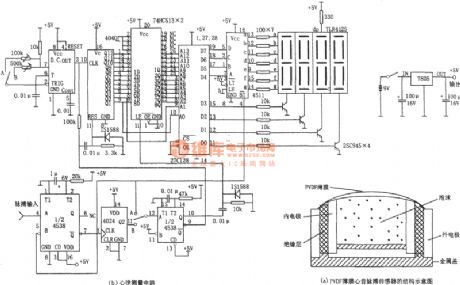
In the figure is the PVD heart sounds impulse measuring circuit. The circuit consists of the single steady oscillator(4538), frequency distributor (4024), pulse generator(ICM7555), counter (4040), storage(ROM), 7-stage lock storage drive(7511),7-stage digital LED and so on. In figure (a) is the PVDF heart sounds impulse sensor structure circuit. For figure (a), PVDF film is a dome shell and it sticks out, so it can contact the earth well. As the PVDF material is soft, which can cling to the skin, its impedance can couple with the skin. (View)
View full Circuit Diagram | Comments | Reading(1543)
The transistor character curve plotter composed of 555
Published:2011/8/14 22:29:00 Author:qqtang | Keyword: transistor character, curve plotter
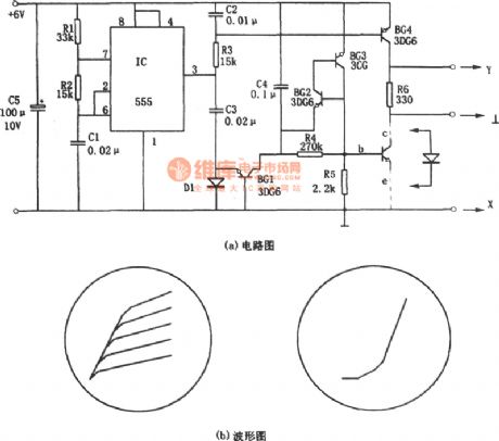
In the figure is the transistor character curve plotter composed of 555. See as figure (a), the circuit consists of the sawtooth wave generator and step wave generator. As it needs two voltages to draw the transistor character, one is the step wave on the b pole, which generates different base currents lb; the other is the sawtooth wave on the c pole, whose period is corresponding to the step wave, so the output character curve of the transistor can be drawn out, i.e Ic-Vce character curve. The sawtooth generator consists of the oscillator (IC(555), R1, R2 and C1) and integral circuit (C2 and R3). (View)
View full Circuit Diagram | Comments | Reading(1047)
| Pages:18/164 1234567891011121314151617181920Under 20 |
Circuit Categories
power supply circuit
Amplifier Circuit
Basic Circuit
LED and Light Circuit
Sensor Circuit
Signal Processing
Electrical Equipment Circuit
Control Circuit
Remote Control Circuit
A/D-D/A Converter Circuit
Audio Circuit
Measuring and Test Circuit
Communication Circuit
Computer-Related Circuit
555 Circuit
Automotive Circuit
Repairing Circuit