
Automotive Circuit
Index 11
Mazda transmission circuit diagram (CALIFORNIA)
Published:2011/9/14 2:08:00 Author:Ecco | Keyword: Mazda transmission , CALIFORNIA
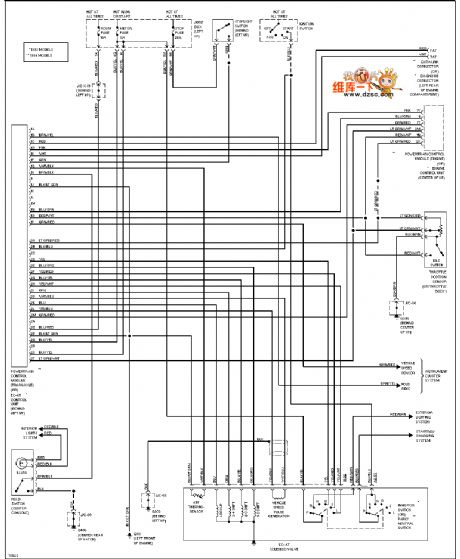
View full Circuit Diagram | Comments | Reading(605)
Mazda starter circuit diagram (AT)
Published:2011/9/14 2:01:00 Author:Ecco | Keyword: Mazda starter, AT
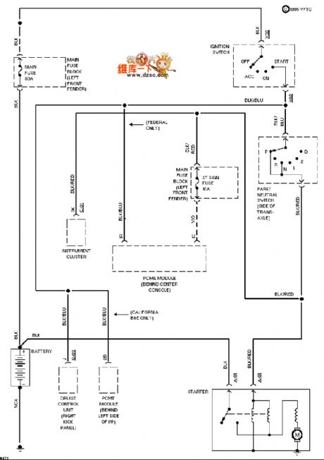
View full Circuit Diagram | Comments | Reading(953)
Low frequency compensation circuit of current transformer
Published:2011/9/15 0:02:00 Author:Sophia | Keyword: Low frequency compensation, current transformer
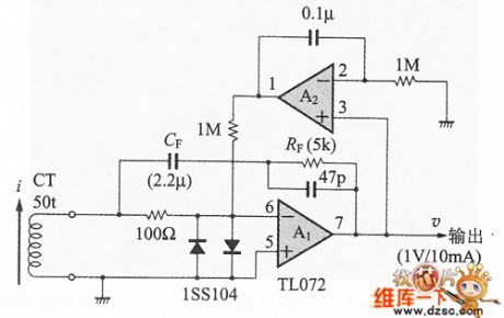
Figure 1 shows the circuit, when the OP amplifier A as the current is inputed into amplifier and visible load resistance R of CT is 0. This circuit can significantly improve the low frequency characteristics. When the gain of low-frequency domain needs to be compensated, the feedback capacitor CF can be inserted into . In this circuit, to prevent the OP amplifier A becoming into open-loop in the DC area and composing of the DC open-loop (fc ≈ 1.6Hz) in the non-inverting integrator A2 (commonly known as the DC servo circuit), this circuit's output voltage v is:
If RF = 50kΩ, then i = 10mA, which can be transformed as 1V.
The value of this capacitor CF is decided by the CF characteristics of short-circuit, so it can be obtained by the experiment. The 47pF capacitor parallelling with FR is to suppress high-frequency characteristics, no special basis. (View)
View full Circuit Diagram | Comments | Reading(5442)
Circuit of Direct Current Motor Driven by SA60
Published:2011/9/15 0:11:00 Author:Zoey | Keyword: Direct Current, Motor, Carrier frequency
The following picture shows the typical connection circuit of direct current motor driven by SA60. Therein, the chip has been connected to an annalog input circuit. A capacitor is connected between numerical input terminal(pin 2) and analog site. By changingthe capacity, frequency of PWM load can be adjusted, making it range between 22 to 250 kHZ. (View)
View full Circuit Diagram | Comments | Reading(612)
simple VSP3010 equivalent input circuit
Published:2011/9/15 1:43:00 Author:chopper | Keyword: simple, equivalent input
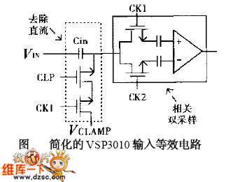
VSP3010 is one of appropriative integrated chips thatare produced by company Burr-Brown and it is used to process CCD signals.It can process signals from channel 1 or channel 3.Each channel has the capability of signal sampling,black level adjustment and programmable gain amplification and then enter 12-bit A/ D whose sampling rate is 12 MHz through multiple selector.Its single-channel signal processing circuit is as following picture. (View)
View full Circuit Diagram | Comments | Reading(668)
HST Hall sensor common application interface circuit
Published:2011/9/14 21:02:00 Author:John | Keyword: sensor, application interface
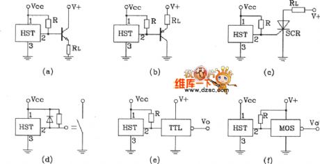
View full Circuit Diagram | Comments | Reading(1700)
Insulation drive circuit with pulse transformer
Published:2011/9/14 6:00:00 Author:Sophia | Keyword: Insulation drive circuit, pulse transformer
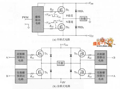
Figure 1 shows that in the half-bridge and full bridge circuit of power MOSFET, how the high-pressure side switch changes to a key point.
Generally, to drive the high-pressure side of the component, a source is required between the gate pole and electrodeinsulation. If it is low-speed switch, as shown in Figure 2 dedicated driver IC constituted by the optical coupler can be used, the source terminal of the high-pressure side will make high-frequency voltage source overlap, and noise is very weak.
Therefore, In reality there are many insulation ways useing the pulse transformer insulation, but to use the pulse transformer,we need to make effor to make the circuit. (View)
View full Circuit Diagram | Comments | Reading(1342)
Working Circuit of the Wiper, Air-heater, Radio and Tape Player of City Hunters in Beijing——2020SG Cross-country Car
Published:2011/9/13 23:56:00 Author:Zoey | Keyword: Working Circuit , wiper, air-heater, Radio and Tape Player, 2020SG Cross-country car
1 Cassette players A BJ20205G4x4 light off-road car is equipped with a stereo cassette player and two speakers 26 and 28, when the ignition switch is in the Ⅰ, Ⅲ position, d can be used.2 Cigarette LighterThe dashboard cigarette lighter 16 ison the left of glove compartment, when lightint the cigarettes, it should be pressed first, when its automatic pop-up (power), they can used, be careful and do nottouchthe heated position of the cigarette lighter.
23 - heater motor; 23, - defrost switch; 24 - washing pump; 24- - wiper switch (including washing switch); 25 - wiper motor; 26 - cassette players; 27 one day line; 28 - speaker; 29, 30 - air fog lights; 31 - fog lamp switch; 32,33 - brake light; 34 - brake light switch; 35 - fl
(View)
View full Circuit Diagram | Comments | Reading(487)
Circuit of Direct Current Motors Driven by LMD18245
Published:2011/9/13 23:49:00 Author:Zoey | Keyword: Direct Current, Motors, Continuous Current
Although the index input bycontinuous current of LMD 18245 is less than 1/3 of SA60, it can adopt various connection methods to control the motor in different ways, so as to get different control performances. Following picture shows the motors example driven by bipolar input. Therein , the chopping time is 1.1RC. RW refers to the current sensor resistance.
UREF is the reference voltage of D/A inverted circuit, D is the input voltage of D/A inverted voltage.IS is the maxmium current of the motor. Distinguished from SA60, there is no PWM circuit in the LMD 18245 Chip. An exterior contrller is needed to control the rotation speed and rotation direction through the duty cycle of PWM. The connection method has been presented in following picture.
(View)
View full Circuit Diagram | Comments | Reading(660)
PLL Composite Oscillator Circuit Composed of CD4046
Published:2011/9/14 10:09:00 Author:Joyce | Keyword: PLL , Composite Oscillator
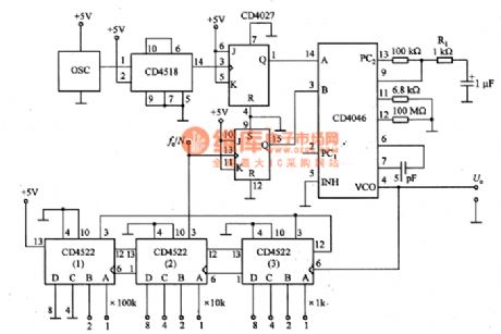
This is a PLL composite oscillator composed of CD4046. It constitutes of reference oscillator, phase comparator, loop filter, voltage-controlled oscillator and programmable frequency divider etc. The reference oscillator can divide the frequency of the output of crystal oscillator module OSC which is 1MHZ or 100 kHz to get a signal of 1 kHz. Then the signal will be compared by CD4046 with the output of frequency dividing circuit N. There are two phase comparators: PC1 and PC2 within CD4046. PC1 is XOR logic, and the duty ratio of output of A and B must be 1:1. (View)
View full Circuit Diagram | Comments | Reading(7669)
the circuit of the constant temperature controller for fish breeding part1
Published:2011/9/12 21:49:00 Author:Ariel Wang | Keyword: constant temperature, controller, fish breeding
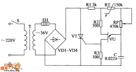
When the temperature of water is beyond the set temperature,the resistence of RT increases.It delays the time when VU outputs the trigger pulse in unit time.The conduction angle of VT decreases.The working voltage of EH decreases.The temperature of water decreases slowly.When the temperature of water is lower than the set temperature,VU outputs trigger pulse earlier.The conduction angle of VT increases.The working voltage of EH increases.The temperature of water goes up.It goes on and on.The water temperature of fish pool stays normal.
(View)
View full Circuit Diagram | Comments | Reading(904)
Inverter home electrotherapy
Published:2011/9/12 21:47:00 Author:Ariel Wang | Keyword: Inverter, home electrotherapy
The home electrotherapy has the the output frequency function of more than ten-speed automatic loop ransformation .The pulse intensity and the speed of the frequency conversion can be adjusted freely.It outputs a broad spectrum.The broad spectrum is very suitable to be as the massor .And it can dissipate fatigue and to be as an adjuvant treatment of some common diseases. The circuit consists of the variable frequency pulse oscillator, the oscillation frequency conversion controller and the pulse output circuit.
(View)
View full Circuit Diagram | Comments | Reading(2184)
LM101A and LM108 high-speed integrator circuit diagram
Published:2011/9/13 6:49:00 Author:Vicky | Keyword: high-speed integrator circuit
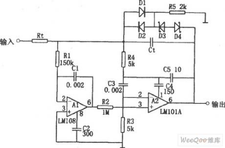
The above picture is a high-speed integrator circuit. The integration time constant RtCt in the circuit has a wide range of changing. In regardless of integration capacitance Ct, A2 is a broadband AC amplifier of positive and negative compensation. When capacitance Ct is added to the negative feedback circuit of A2, then the integrator comes into being. Because the low frequency and DC part of input signal are added to the non-inverting input end of A2 via A1 and resistance R2 respectively, the high-speed integrator then is formed, and it allows relatively low input bias current. Positive and negative compensation is composed of R4, C4 and C5. (View)
View full Circuit Diagram | Comments | Reading(1562)
Square Wave Turning Triangular Wave Circuit
Published:2011/9/12 23:49:00 Author:Sue | Keyword: Square Wave, Triangular Wave
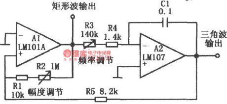
The picture shows the oscillating circuit with triangular wave and square wave output. The circuitconsists of Miller integrator A2 and Schmitt trigger A1, which can generate triangular wave and square wave output.The oscillation frequency is determined by Miller integrator's time constant (R3+R4)C1 and trigger's lagging voltage Vcc(R1+R2)/(R1+R2+R3), and the Vcc is power voltage.By adjusting the resistor R3, the oscillation frequency can be changed. By adjusting the resistor R2, the triangular wave's outputlatitude can be changed and the oscillation frequency can also be changed. (View)
View full Circuit Diagram | Comments | Reading(942)
Retractable Dot Display Level Indicator Composed of SL322
Published:2011/9/12 23:49:00 Author:Sue | Keyword: Retractable, Dot Display, Level Indicator
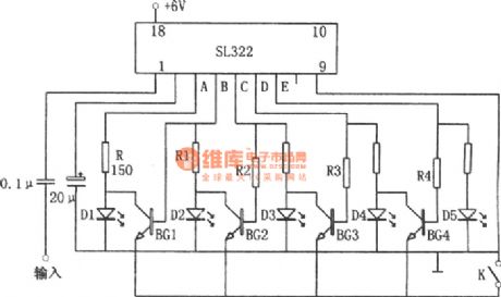
The picture shows the retractable dot display level indicator circuit. The circuit consists of luminescent display drive SL322, LED D1-D5, transistor BG1-BG5. When K is disconnected, the triodes are all connected to the ground. When the level becomes higher which makes the LED D2 illuminated, B's level becomes higher and BG1 is connected which will make the LED D1 off. When the level becomes higher which makes D3 illuminated, C's level becomes higher which makes BG2 connected, and D2 will be off. At this time, B's level doesn't change and BG1 remains disconnected. D1 is still not illuminated. (View)
View full Circuit Diagram | Comments | Reading(774)
Circuit diagram of multi-vibrator composed by triodes
Published:2011/9/7 3:48:00 Author:Vicky | Keyword: multi-vibrator, triode
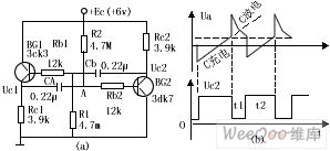
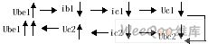
The above picture is a multi-vibrator composed by triodes. The circuit is still composed of phase inverter coupling by two-polar base resistance-capacity. When the circuit power is on, the two tubes cannot be conducted at once, because the charging route for CA is: Ec→R2→CA→Rc1; the charging route for CB is : Ec→Rc2→CB→R1. When CA and CB are charged to a certain value, UCA and UCB , as the forward bias voltage of tube base loop, make Ib1 and Ib2 increase. Due to the performance of positive feedback, the BG1 and BG2 soon becomes saturation. This is a temporarily-stable state.
Once the saturation starts, CA discharges via emitter framework of Rb2, BG2 and resistance Rc1. (View)
View full Circuit Diagram | Comments | Reading(1010)
8-Channel Digital Display Responder Composed of CH233 And 74LS273
Published:2011/8/25 7:41:00 Author:Sue | Keyword: 8-Channel, Digital Display, Responder
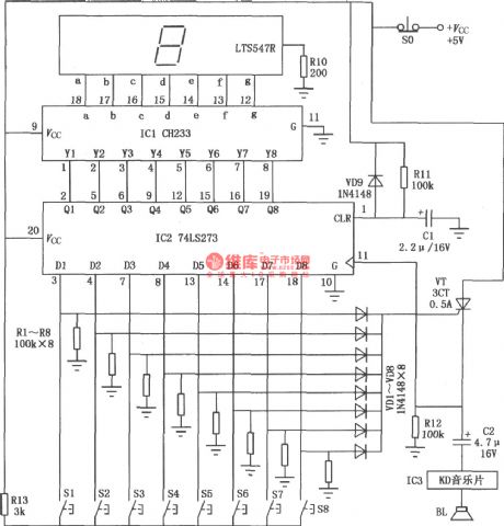
The picture shows the 8-channel digital display responder which is composed of CH233 and 74LS273. (View)
View full Circuit Diagram | Comments | Reading(2688)
Logic Display Pen Circuit with 4 States Composed of CD4511
Published:2011/8/25 7:48:00 Author:Sue | Keyword: Logic Display Pen, 4 States
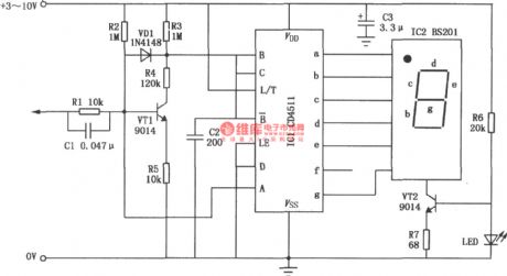
The picture shows the logic display pen circuit with 4 states composed of CD4511. (View)
View full Circuit Diagram | Comments | Reading(4393)
Voltage Control Oscillator with Automatic Trace-Frequency-Way Composed of MC34025P
Published:2011/8/25 7:48:00 Author:Sue | Keyword: Voltage Control, Oscillator, Automatic Trace-Frequency-Way
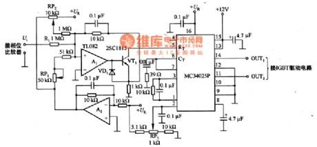
The picture shows the voltage control oscillator with automatic trace-frequency-way composed of MC34025P. The circuit can be used as voltage control oscillator with automatic trace-frequency-way in ultrasonic oscillator. The output circuit of the ultrasonic oscillator is half-bridge way, so the power integrated circuit uses MC34025P which is two-phase output.
MC34025P has a wide oscillation frequency which is between 15 to 50KHZ. The center frequency is set by RP1, RP2. RP3 sets duty ratio which can prevent the push-pull switch circuit's two transistors from being connected at the same time. (View)
View full Circuit Diagram | Comments | Reading(1166)
Four-order Low-pass Filter Circuit without Capacity Cell
Published:2011/8/25 7:48:00 Author:Sue | Keyword: Four-order, Low-pass, Filter, without Capacity Cell
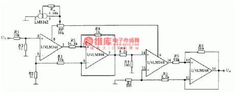
The picture shows the four-order low-pass filter circuit without capacity cell. (View)
View full Circuit Diagram | Comments | Reading(664)
| Pages:11/164 1234567891011121314151617181920Under 20 |
Circuit Categories
power supply circuit
Amplifier Circuit
Basic Circuit
LED and Light Circuit
Sensor Circuit
Signal Processing
Electrical Equipment Circuit
Control Circuit
Remote Control Circuit
A/D-D/A Converter Circuit
Audio Circuit
Measuring and Test Circuit
Communication Circuit
Computer-Related Circuit
555 Circuit
Automotive Circuit
Repairing Circuit