
Automotive Circuit
Index 17
The electronic sphygmograph
Published:2011/8/23 1:01:00 Author: | Keyword: electronic , sphygmograph
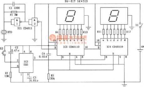
The electronic sphygmograph is shown as the chart.It converts the change of pulse pressure to electric signal through the sensor.Then it is handled by enlarging,shaping,counting, coding and driving.Finally the digitron displays how many times a minute your pulse is pulsing.It is very convenient to use.
(View)
View full Circuit Diagram | Comments | Reading(805)
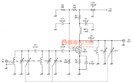
the amplier circuit of the radio frequency :Dual-gate MOSFET RF amplifier circuit
Published:2011/8/22 21:35:00 Author: | Keyword: amplier, Dual-gate , MOSFET, RF, amplifier
View full Circuit Diagram | Comments | Reading(3765)
The regulator: DC-DC circuit, power supply monitor pin and its main features L78LR05
Published:2011/8/30 0:20:00 Author:Seven | Keyword: DC-DC circuit, power supply, monitor pin
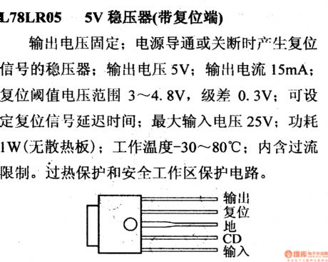
L78LR05--the 5V stabilizer (with reset terminal)The output voltage is fixed; it is a stabilizer which generates the stable reset signal when the power is put through or broken down; the output voltage is 5V; the output current is 15mA; the reset threshold voltage range is 3~4.8V, the stage difference is 0.3V; the reset signal time delay can be set; the max input voltage is 25V; the power consumption is 1W(without any radiator); the working temperature is -30~80℃; it contains the over-current limitation, over-heat protection and secure working area protection circuit.
(View)
View full Circuit Diagram | Comments | Reading(662)
The regulator: DC-DC circuit, power supply monitor pin and its main features IR3M01
Published:2011/8/29 23:47:00 Author:Seven | Keyword: DC-DC circuit, power supply, monitor pin
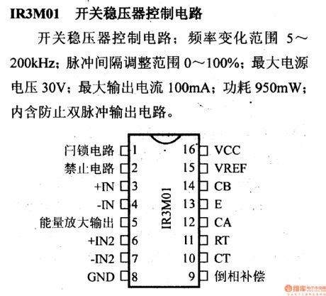
IR3M01--the switch stabilizer control circuitThis is a switch stabilizer control circuit; the frequency range is 5~200kHz; the pulse interval adjustment range is 0~100%; the max power supply voltage is 30V; the max output current is 100mA; the power consumption is 950mW; it contains the anti-dual-pulse output circuit.
(View)
View full Circuit Diagram | Comments | Reading(1342)
The regulator: DC-DC circuit, power supply monitor pin and its main features HA16666FP/16666PS
Published:2011/8/30 0:12:00 Author:Seven | Keyword: DC-DC circuit, power supply, monitor pin
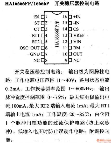
HA16666FP/16666PS--the switch stabilizer control circuitThis is a switch stabilizer control circuit; the output stage is the totem pillar circuit; the working power supply voltage range is 11~40V; the standby state current is 0.3mA; the working oscillating frequency range is 1~600kHz; the output pulse width control range is 0~75%; the max electrode output current is 100mA; the max RT2 terminal input current is 1mA; the max RT1 terminal output current is 1mA; the working temperature is -20~85℃; it contains a pulse latch over-current protection circuit(to avoid dual pulse) and low input voltage mistake prevention circuit; it has the remote control function. (View)
View full Circuit Diagram | Comments | Reading(651)
The regulator: DC-DC circuit, power supply monitor pin and its main features DS1836A/B/C/D
Published:2011/8/29 23:41:00 Author:Seven | Keyword: DC-DC circuit, power supply, monitor pin
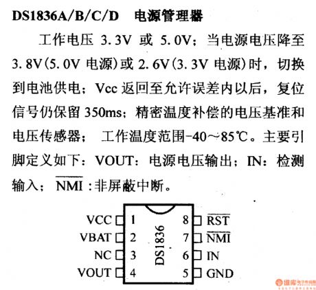
DS1836A/B/C/D--the power supply managerThe working voltage is 3.3V or 5.0V; when the power supply voltage drops to 3.8V (5.0V power supply) or 2.6V (3.3V voltage), it is powered by the battery; after the Vcc turns back to the allowed fault range, the reset signal remains 350ms; the voltage reference and voltage sensor are precisely compensated; the working temperature range is -40~85℃. The definitions of its features are as follows: VOUT: the power supply voltage output; IN: test input.
(View)
View full Circuit Diagram | Comments | Reading(644)
The regulator: DC-DC circuit, power supply monitor pin and its main features IR9494
Published:2011/8/29 23:52:00 Author:Seven | Keyword: DC-DC circuit, power supply, monitor pin
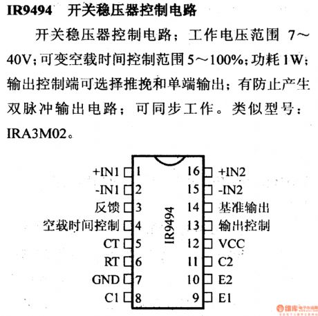
IR9494--the switch stabilizer control circuitThis is a switch stabilizer control circuit; its working voltage range is 7~40V; the control range of changeable empty load time is 5~100%; the power consumption is 1W; the output control terminal can be the push-pull or single terminal output; it contains the output circuit which prevents the dual pulse; it can work synchronously. The approximate type is IRAM02.
(View)
View full Circuit Diagram | Comments | Reading(874)
The regulator: DC-DC circuit, power supply monitor pin and its main features IR9431
Published:2011/8/30 0:03:00 Author:Seven | Keyword: DC-DC circuit, power supply, monitor pin
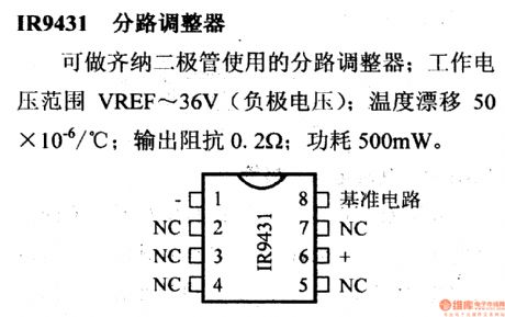
IR9431--the distributing regulatorIt can be the distributing regulator of the Zener diode; the working voltage range is VREF~36V(negative pole voltage); the temperature drift is 50*10-6/℃; the output impedance is 0.2Ω; the power consumption is 500mW.
(View)
View full Circuit Diagram | Comments | Reading(842)
The regulator: DC-DC circuit, power supply monitor pin and its main features IR3M03A
Published:2011/8/29 23:59:00 Author:Seven | Keyword: DC-DC circuit, power supply, monitor pin
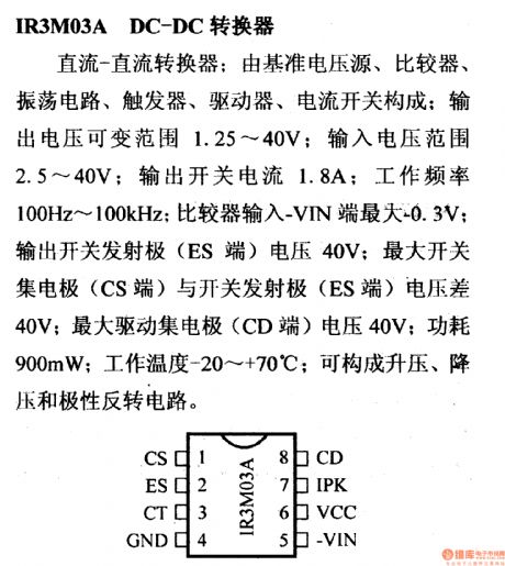
IR3M03A--the DC-DC converterThis is a DC-DC converter which consists of the Vref source, comparator, oscillator circuit, trigger, driver and current switch; the output voltage changeable range is 1.25~40V; the input voltage range is 2.5~40V; the output switch current is 1.8A; the working frequency is 100Hz~100KHz; the MAX voltage of comparator input-VIN terminal is -0.3V; the voltage of the output switch emitter (ES terminal) is 40V; the max switch electrode (CS terminal) and the switch emitter (ES terminal) has a voltage difference of 40V; the max drive electrode (CD terminal) voltage is 40V.
(View)
View full Circuit Diagram | Comments | Reading(1575)
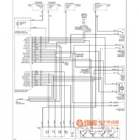
Buick ant-locking braking circuit diagram
Published:2011/8/19 0:48:00 Author:Jessie | Keyword: Buick , ant-locking braking circuit
View full Circuit Diagram | Comments | Reading(651)
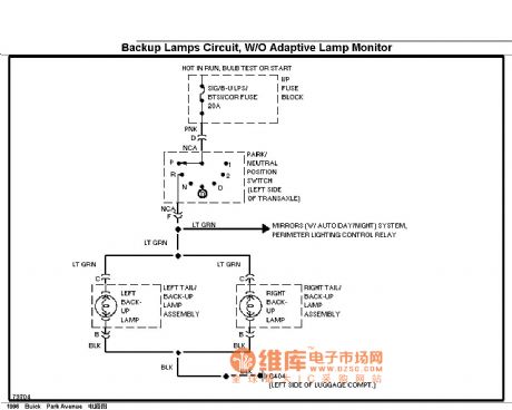
Buick reversing light circuit diagram( without light dimming control)
Published:2011/8/19 0:49:00 Author:Jessie | Keyword: Buick , reversing light , light dimming control
View full Circuit Diagram | Comments | Reading(616)
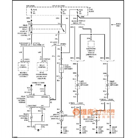
Buick demisting circuit diagram(demisting boneville wc61)
Published:2011/8/19 0:50:00 Author:Jessie | Keyword: Buick, demisting, boneville wc61
View full Circuit Diagram | Comments | Reading(679)
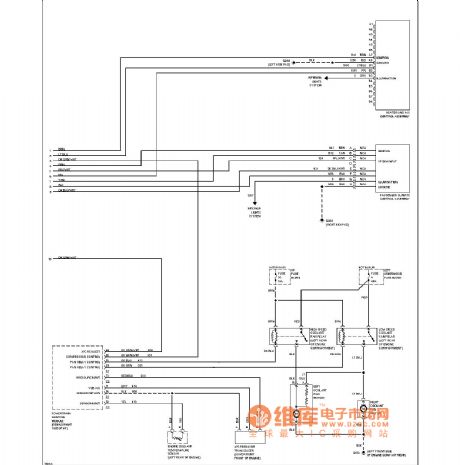
Buick air conditioning circuit diagram(automatic air conditioning)
Published:2011/8/19 1:02:00 Author:Jessie | Keyword: air conditioning , automatic, Buick
View full Circuit Diagram | Comments | Reading(1208)
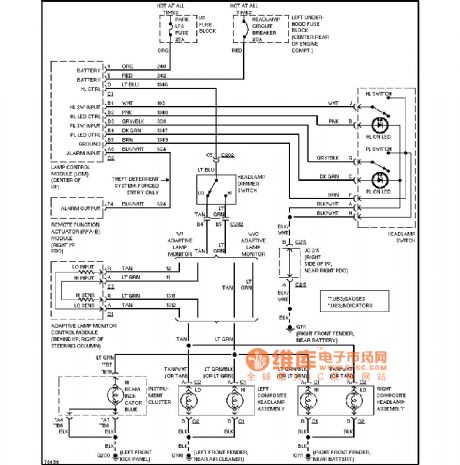
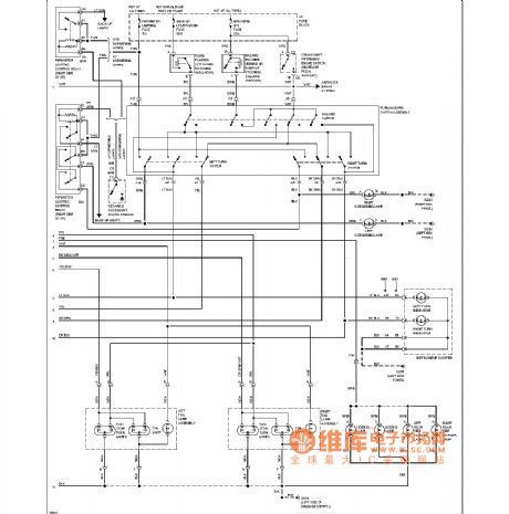
Buick headlamp circuit diagram(no DRL, with beam adjustment)
Published:2011/8/18 22:55:00 Author:Jessie | Keyword: Buick headlamp , no DRL, beam adjustment
View full Circuit Diagram | Comments | Reading(719)
Buick power supply circuit diagram
Published:2011/8/18 2:17:00 Author:Jessie | Keyword: Buick power supply
View full Circuit Diagram | Comments | Reading(625)
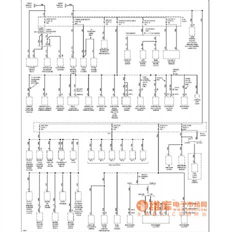
Buick transmission circuit diagram(3.8l,vin1)
Published:2011/8/17 22:04:00 Author:Jessie | Keyword: transmission , 3.8l,vin1, Buick
View full Circuit Diagram | Comments | Reading(580)
Buick backup lamp circuit diagram( with light dimming control)
Published:2011/8/18 0:53:00 Author:Jessie | Keyword: Buick , backup lamp, light dimming control
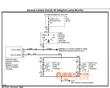
View full Circuit Diagram | Comments | Reading(639)
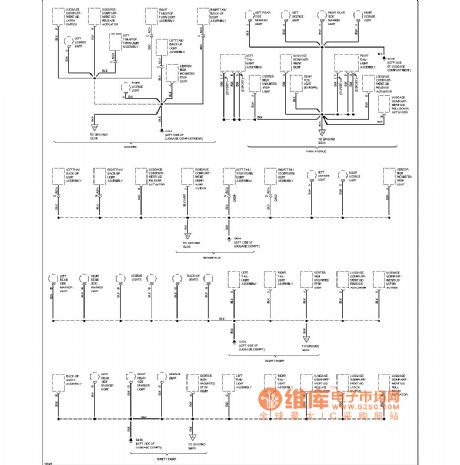
Buick external light circuit diagram( with light dimming control)
Published:2011/8/18 0:55:00 Author:Jessie | Keyword: Buick , external light, light dimming control
View full Circuit Diagram | Comments | Reading(619)
Buick put up iron distribution circuit diagram
Published:2011/8/17 22:01:00 Author:Jessie | Keyword: Buick , put up iron distribution
View full Circuit Diagram | Comments | Reading(627)
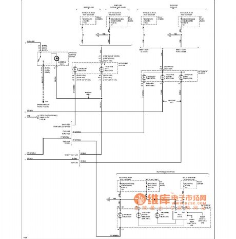
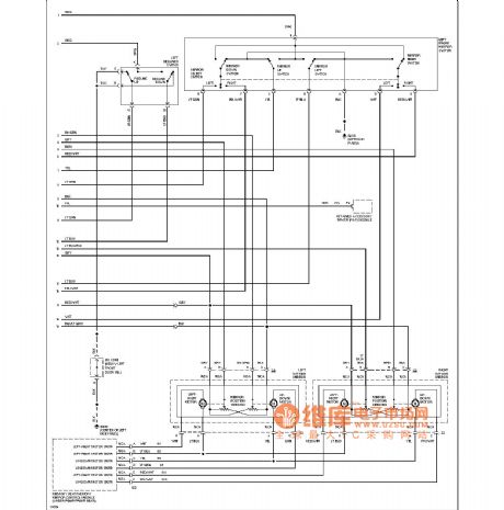
Buick automatic memory seats and rearview mirror circuit diagram
Published:2011/8/17 21:44:00 Author:Jessie | Keyword: automatic memory seats, rearview mirror
View full Circuit Diagram | Comments | Reading(550)
| Pages:17/164 1234567891011121314151617181920Under 20 |
Circuit Categories
power supply circuit
Amplifier Circuit
Basic Circuit
LED and Light Circuit
Sensor Circuit
Signal Processing
Electrical Equipment Circuit
Control Circuit
Remote Control Circuit
A/D-D/A Converter Circuit
Audio Circuit
Measuring and Test Circuit
Communication Circuit
Computer-Related Circuit
555 Circuit
Automotive Circuit
Repairing Circuit