
Index 192
VFC100 synchronizing voltage / frequency converter circuit
Published:2011/7/26 6:28:00 Author:Fiona | Keyword: synchronizing voltage / frequency, converter
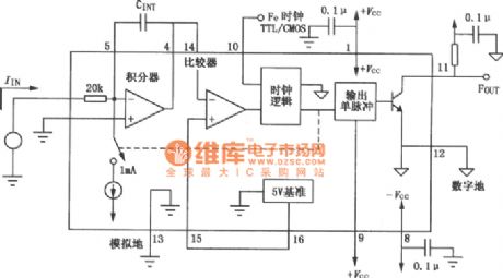
VFC100 is asynchronizing voltage / frequency converter which has strong function and it uses charge balance technology.Strict reset combined cycle is from the external clock frequency,it can better eliminate errors and the external timing components' drifting required by other converters. It also uses high-precision input resistor to set full scale input voltage,in many applications,it can obtain the required accuracy without external adjustment.Its typical application circuit is shown as above.
(View)
View full Circuit Diagram | Comments | Reading(800)
Trigger Circuit of Devices
Published:2011/7/16 0:41:00 Author:Felicity | Keyword: Trigger
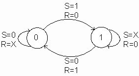
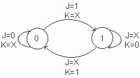
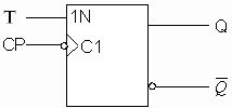
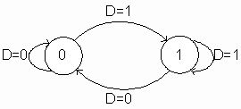
We have three ways to describe the logical function of trigger. First is characteristic equation. Second is characteristic table and the third one is state transition diagram. (showed in picture 1,2,3,4)
Picture 1 shows the state transition diagram of RS Trigger.
Picture2 shows the state transition diagram ofJK Trigger.
Picture3 shows the state transition diagram and logical symbol ofJK Trigger.
Picture4 shows the state transition diagram ofD Trigger.
Characteristics table is actually a special kind of truth table and it has a very specific description of trigger.The input variables (independent variables)of truth table are not only data entry but also initial states of flip-flop. And the output variable (dependent variable) is the next state flip-flop. Characteristic equation is out from the feature table summarizes so it's more concise. State transition diagramwhich describes the methodsis very intuitive. (View)
View full Circuit Diagram | Comments | Reading(805)
Coded lock (CD7556) circuit only using one button
Published:2011/7/20 20:26:00 Author:Fiona | Keyword: one button, Coded lock
View full Circuit Diagram | Comments | Reading(761)
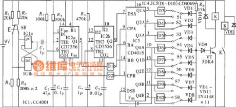
Nine digital password controller circuit composed of CD4017
Published:2011/7/20 20:29:00 Author:Fiona | Keyword: Nine digital password, controller
View full Circuit Diagram | Comments | Reading(1147)
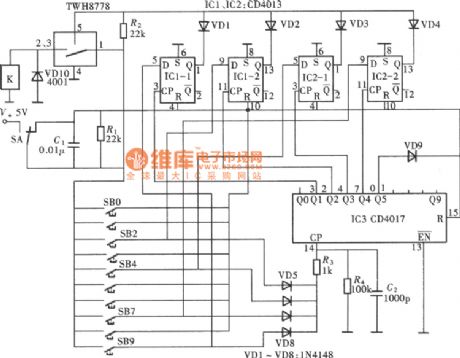
Ten digital password switch (CD4013,CD4017) circuit
Published:2011/7/20 20:31:00 Author:Fiona | Keyword: Ten digital password switch
View full Circuit Diagram | Comments | Reading(3080)
Ten key password switch (CD4066,CD4043) circuit
Published:2011/7/20 20:32:00 Author:Fiona | Keyword: Ten key password switch
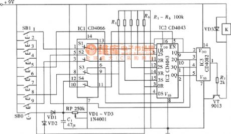
View full Circuit Diagram | Comments | Reading(4121)
The coded lock (CD4017,CD4093) circuit which can identify the pseudo code
Published:2011/7/20 20:34:00 Author:Fiona | Keyword: coded lock, identify the pseudo code
View full Circuit Diagram | Comments | Reading(3220)
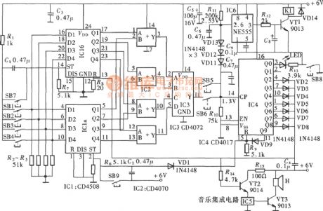
The coded lock having the alarm function (CD4508,CD4070,CD4017,CD4072) circuit
Published:2011/7/20 20:36:00 Author:Fiona | Keyword: coded lock, the alarm function
View full Circuit Diagram | Comments | Reading(3544)
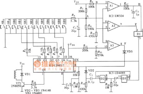
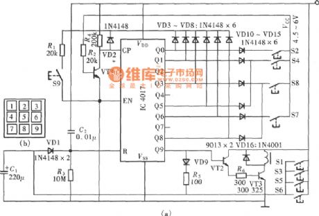
The password switch having the alarm function (CD4017,CD4013) circuit
Published:2011/7/20 20:38:00 Author:Fiona | Keyword: password switch, the alarm function
View full Circuit Diagram | Comments | Reading(1567)
Four ways of input/output audio switch (CD4017, CD4066) circuit
Published:2011/7/20 20:03:00 Author:Fiona | Keyword: Four ways of input/output, audio switch
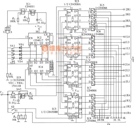
View full Circuit Diagram | Comments | Reading(4779)
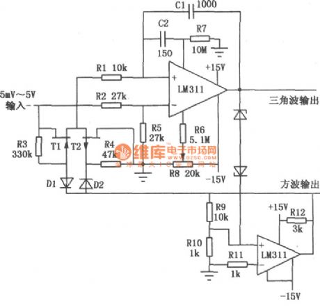
The typical application circuit of LM111/211/311
Published:2011/7/20 20:08:00 Author:Fiona | Keyword: typical application

View full Circuit Diagram | Comments | Reading(939)
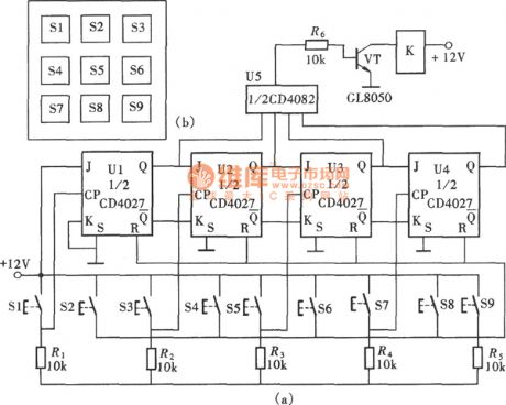
Nine key coded lock circuit composed of CD4027
Published:2011/7/20 20:20:00 Author:Fiona | Keyword: Nine key coded lock
View full Circuit Diagram | Comments | Reading(1356)
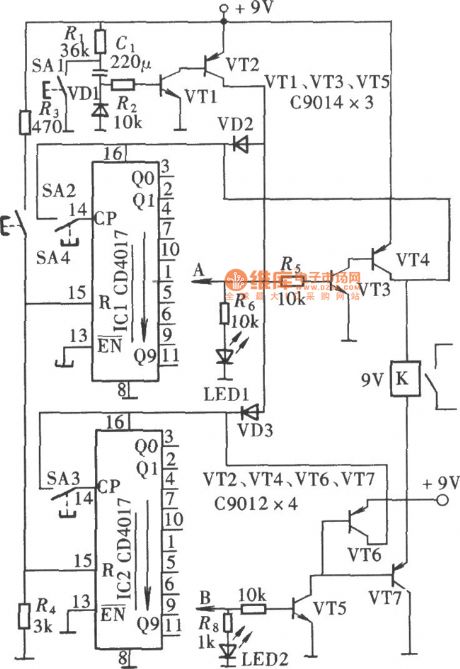
Time-control type coded lock circuit composed of CD4017
Published:2011/7/20 20:20:00 Author:Fiona | Keyword: Time-control type, coded lock
View full Circuit Diagram | Comments | Reading(654)
Nine key coded lock circuit composed of CD4017
Published:2011/7/20 20:21:00 Author:Fiona | Keyword: Nine key, coded lock
View full Circuit Diagram | Comments | Reading(1034)
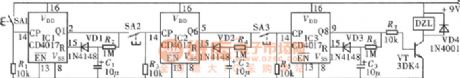
Safe and reliable coded lock (CD4017) circuit
Published:2011/7/20 20:23:00 Author:Fiona | Keyword: Safe and reliable, coded lock
View full Circuit Diagram | Comments | Reading(1072)
Super coded lock circuit composed of CD4017
Published:2011/7/20 20:24:00 Author:Fiona | Keyword: Super coded lock
View full Circuit Diagram | Comments | Reading(768)
VFC62 voltage / frequency,frequency / voltage converter circuit
Published:2011/7/21 3:37:00 Author:Fiona | Keyword: voltage / frequency, frequency / voltage, converter

VFC62 voltage / frequency,frequency / voltage converter can easily convert analog signals into digital signals.The digital output uses the form of open collector,digital pulse repetition rate is proportional to the amplitude of the input analog voltage,the output pulse level is compatible with DTL,TTL and CMOS logic family.As shown in figure is its typical application circuit.
(View)
View full Circuit Diagram | Comments | Reading(4657)
Electric fence control circuit 5
Published:2011/7/25 2:50:00 Author:Ecco | Keyword: Electric fence control
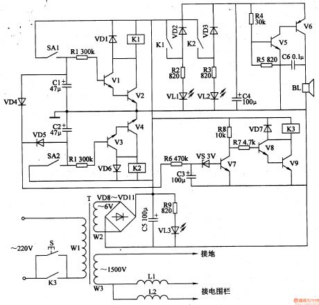
The electric fence control circuit is composed of the +6 V power supply circuit, high-voltage output circuit, trigger control circuit, alarm circuit and protection circuit, and it is shown in Figure 4-30. +6 V power supply circuit is composed of the power control button S, power transformer T, rectifier diodes VD8-VDll, filter capacitor C5, current-limiting resistor R9 and the power indicator LED VL3. Trigger control circuit consists of reeds SAl, SA2, resistors Rl, RlO, diodes VDl, VD6, transistors Vl-V4 and relays Kl, K2.
(View)
View full Circuit Diagram | Comments | Reading(3759)
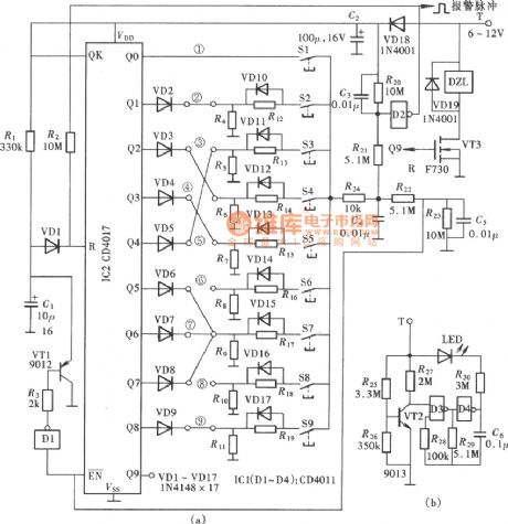
Electric fence control circuit 4
Published:2011/7/25 2:47:00 Author:Ecco | Keyword: Electric fence control
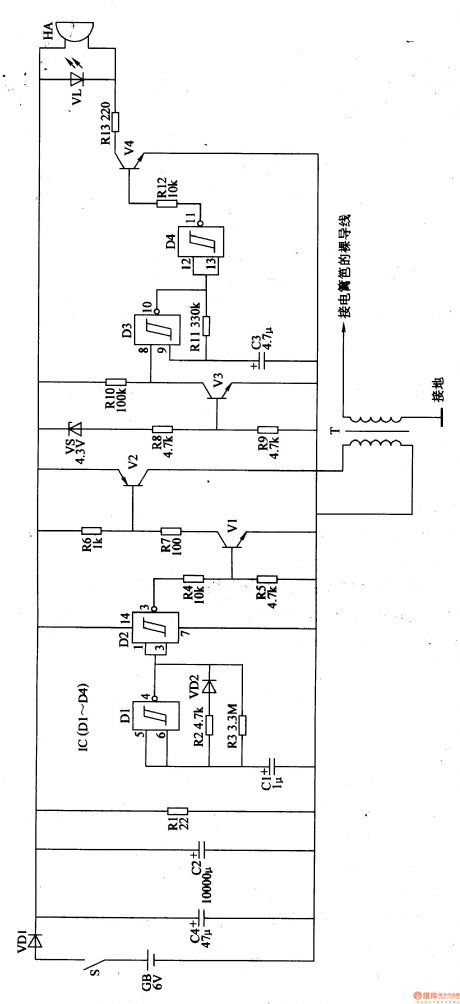
The electric fence control circuit is composed of the pulse generator, high-voltage generator and undervoltage alarm circuit, and it is shown in Figure 4-29. Pulse generator circuit consists of the Dl, D2 which are inside of NAND gate Schmitt trigger IC (Dl-D4), resistors R2, R3, and capacitor Cl, diode VD2. High-voltage generator circuit is composed of the R4-R7, transistors Vl, V2, and pulse transformer T. Undervoltage alarm circuit is composed of the internal D3, D4 of IC, transistors V3, V4, voltage regulator diode VS, resistors R8-R13, capacitor C3, light emitting diode VL and buzzer HA.
(View)
View full Circuit Diagram | Comments | Reading(2414)
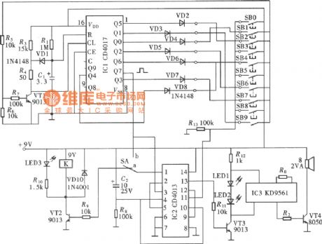
The control switch circuit with the cd4017
Published:2011/7/25 2:26:00 Author:Christina | Keyword: control switch
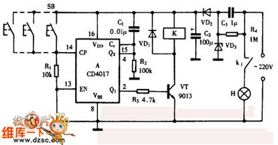
The output port q2 of cd4017 is connected with the clear port cr, so the q0 and q1 outputs the high level alternately under the function of the cp port input pulse. When the power is connected, the pin-15's differential circuits r2 and c1 clear the circuit, the q0 port outputs the high level, the q1 port outputs the low level, the transistor vt cuts off, the relay k will not operate, the light h which is controlled by k will not turns on. If you press the button sb which is connected with cp in parallel, the cp port will output a positive pulse, the q0 port outputs the low level, q1 outputs the high level, the vt conducts, the relay k gets power to close, the normally open contact point closes, the light h turns on.
(View)
View full Circuit Diagram | Comments | Reading(887)
| Pages:192/312 At 20181182183184185186187188189190191192193194195196197198199200Under 20 |
Circuit Categories
power supply circuit
Amplifier Circuit
Basic Circuit
LED and Light Circuit
Sensor Circuit
Signal Processing
Electrical Equipment Circuit
Control Circuit
Remote Control Circuit
A/D-D/A Converter Circuit
Audio Circuit
Measuring and Test Circuit
Communication Circuit
Computer-Related Circuit
555 Circuit
Automotive Circuit
Repairing Circuit