
Index 190
Division Circuit 5
Published:2011/7/21 8:02:00 Author:Sue | Keyword: Division Circuit
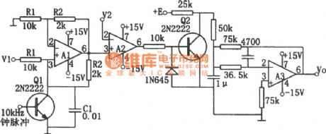
The picture shows division circuit. A1 composes voltage-controlled current source. A2 composes voltage comparator. A3 composes active low pass filter. When the time constant R1C1 is equal to clock pulse period T, the relation of the output and input is: Vo=-V2E/V1. If E is made to be 1V, then Vo=-V2/V1. V1 and V2 are both required to be positive and are restricted within 10V. V2 is a little lower than V1. The resistor R1,R2 and capacitor C1 is required to use components with good temperature stability. A1 is HA2-2520. A2,A3 are LM101A. (View)
View full Circuit Diagram | Comments | Reading(674)
Linear Direct Current Voltage Multiplier(ICL8048,ICL8049) Circuit
Published:2011/7/21 6:16:00 Author:Sue | Keyword: Linear, Direct Current, Voltage, Multiplier
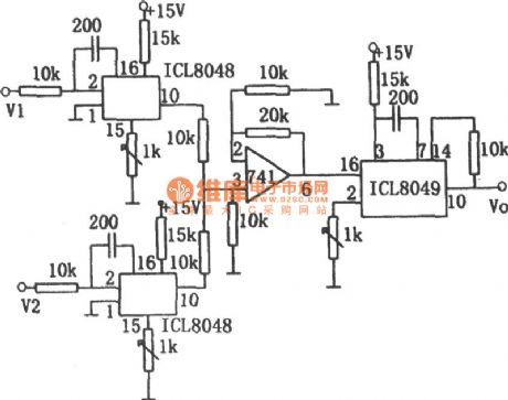
The picture shows the linear direct current voltage multiplier circuit. The circuit uses two ICL8048 logarithmic amplifiers, one antilog amplifier ICL8049 and one 741 operational amplifier. The relation between the output voltage and the two input voltages is: Vo=V1V2/10. In the circuit, V1 and V2 are direct current voltage of +0.1-10V. When the input voltage is +10V, the precision is 1%. (View)
View full Circuit Diagram | Comments | Reading(1493)
Multiplying Circuit Composed of MC1496
Published:2011/7/21 6:40:00 Author:Sue | Keyword: Multiplying Circuit
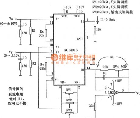
The picture shows the multiplying circuit composed of MC1496. In the circuit, when Rx=30kΩ, Ry=62kΩ,I1=0.5mA,K=1/10, the output voltage Vo=VxVy/10. The output current Io is phase reversed by the inverting amplifier, so Vx is put on X-terminal, and it is decided by that the right side of the formula is positive. If the right side is negative, the input signal should be put on X+terminal. In order to avoid parasitic oscillation, series network composed of 10pF and 470Ω should be connected to the input terminal of Vx and Vy.
RV1=20kΩ, Y is imbalance adjusted.
RV2=20kΩ, X is imbalance adjusted.
RV3=20kΩ, output imbalance adjusted.
When the signal source's direct current resistance value is low, R1 and R2 can be disconnected. (View)
View full Circuit Diagram | Comments | Reading(1304)
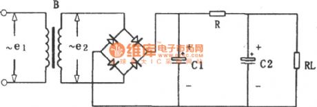
Power Noise Filter Circuit
Published:2011/7/21 7:15:00 Author:Sue | Keyword: Power, Noise, Filter
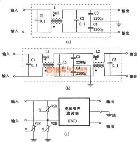
The power noise filter(PNF) is a new type of device which can effectively reduce the alternatingelectric wirenoise andimprove the electric device's capacity of resisting disturbance and the reliability of system. Ithas two functions. On one hand, it can remove or reduce the noise disturbancefrom the alternating current electric wire which will make the electric device work normally. On the other hand, it can prevent the noise generated by the electric device from entering into the electric wire. Many factors can generate high frequency noise disturbance signal on the alternating current electric wire, and the high frequency disturbance signal will enter into the electric device through the power, so it will reduce the noise-signal ratio greatly and there will be nonlinear distortion. (View)
View full Circuit Diagram | Comments | Reading(1861)
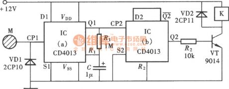
Alternating Current Power Supply Over- And Under-Voltage(CD4013) Circuit
Published:2011/7/23 6:24:00 Author:Sue | Keyword: Alternating Current, Power Supply, Over- And Under-Voltage
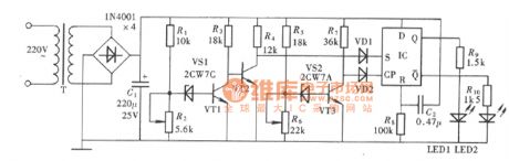
In China, the standard voltage of alternating current power supply is 220V, its maximum allowable deviation range is 180-240V. It the voltage is beyond the allowable range, it will harm the electrical equipment. CD4013 can compose a power supply over- and under-voltage detection circuit. When the power supply's voltage exceeds the range, the detection circuit will send outalarm signal which will warn the users to cut off the power supply or to take some protection measures, so that any losts can be avoided. The picture shows the over- and under-voltage detection circuit. It consists of power supply over- and under-voltage detection and sampling circuit, trigger control and display circuit. (View)
View full Circuit Diagram | Comments | Reading(1200)
Multiplying Circuit Composed of CA309
Published:2011/7/21 5:54:00 Author:Sue | Keyword: Multiplying
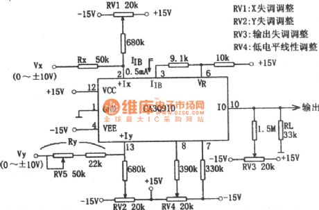
The picture shows the multiplying circuit composed of CA3091. When Rx=50kΩ,Ry=33kΩ, RL=33kΩ, IIB=0.5mA, K= 1/10, the output voltage Vo=VxVy/10.
RV1: X imbalance adjustment.
RV2: Y imbalance adjustment.
RV3: Output imbalance adjustment.
RV4: Low level linear adjustment. (View)
View full Circuit Diagram | Comments | Reading(596)
Jitter Buffer Switch(CD4011,CD4043) Circuit Composed of Gate Circuit
Published:2011/7/21 1:14:00 Author:Sue | Keyword: Jitter Buffer Switch, Gate Circuit
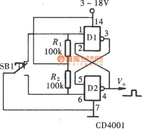
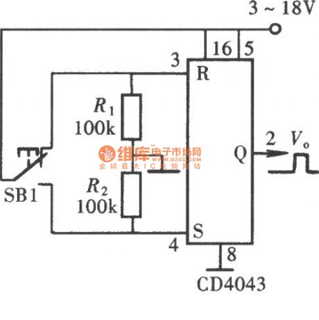
Working principle diagram composed of CD4011:
Working principle diagram composed of CD4043:
(View)
View full Circuit Diagram | Comments | Reading(2563)
Division Circuit Composed of MC1494 and LM307
Published:2011/7/21 6:06:00 Author:Sue | Keyword: Division Circuit
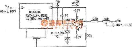
The picture shows division circuit composed of MC1494 and LM307. In the circuit, the output voltage Vo=10Vz/Vx. The input signal Vx and Vz can be either positive and negative, so the circuit is four-quadrant division circuit. The zener diode which is connected to LM307N's input terminal is output voltage's clamping diode when the input Vx is reduced. (View)
View full Circuit Diagram | Comments | Reading(603)
Division Circuit 1(MPY100)
Published:2011/7/21 7:31:00 Author:Sue | Keyword: Division Circuit
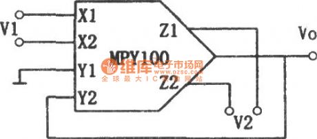
The picture shows the division circuit. The circuit is composed of divider and multiplier integrated circuit MPY100. The input signal is V1,V2. The output Vo=10V2/V1. Such divider is composed by connecting the multiplier to the operational amplifier's return circuit. V1's input range is -0.2V-10V. V2's input range is -10V-10V. When V1 is very small, the circuit's error is large. (View)
View full Circuit Diagram | Comments | Reading(688)
Division Circuit 2(MPY600)
Published:2011/7/21 7:39:00 Author:Sue | Keyword: Division Circuit
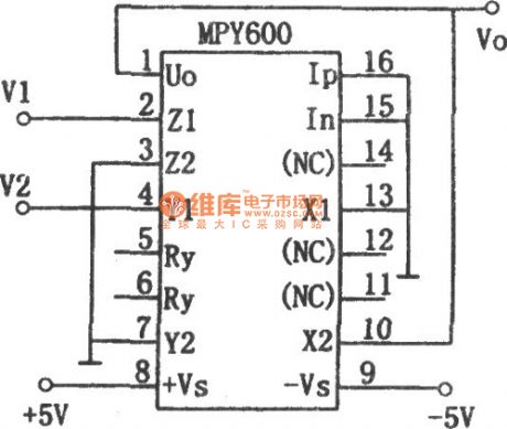
The picture shows the division circuit. It consists of multiplier MPY600. Its input is V1,V2, and the full input range is ±2V. Its output Vo=2V1/V2. When the integrated circuit is used as division application, its band width is related to V2. The larger is V2, the larger is the band width. (View)
View full Circuit Diagram | Comments | Reading(562)
Division Circuit 3(4302)
Published:2011/7/22 8:01:00 Author:Sue | Keyword: Division Circuit
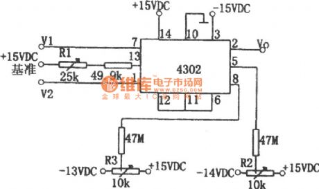
The division circuit shown in the picture consists of integrated block 4302. Its input is V1,V2, and output Vo=10V1/V2. Its input signal range is: 0.03V≤V1≤10V,0.03V≤V2≤10V. When the temperature is 25℃, the typical error is ±25mV, and the maximum error is ±50V. What's more, the output voltage precision is effected by temperature, and its temperature coefficient is ±1mV/C. When the temperature is 25℃, the output offset voltage is ±10mV, and the temperature coefficient is ±1mV/C. (View)
View full Circuit Diagram | Comments | Reading(652)
Electric Relay Circuit Leading Glow Numerating Tube
Published:2011/7/23 5:47:00 Author:Sue | Keyword: Electric Relay, Glow Numerating Tube
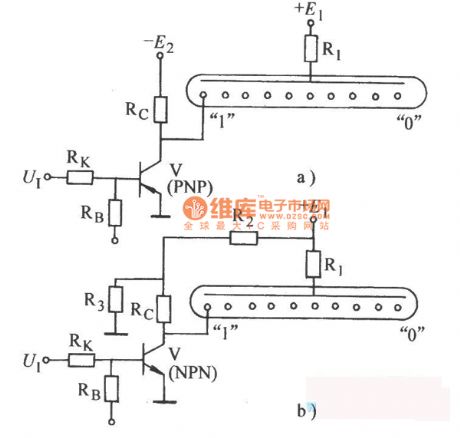
The circuit shown infigure a) is used in zero negative logic system.
The circuit shown in figure b) is used in zero positive logic system. (View)
View full Circuit Diagram | Comments | Reading(546)
Multi-channel Multi-state Control Switch Composed of CD4017
Published:2011/7/22 5:26:00 Author:Sue | Keyword: Multi-channel Multi-state Control Switch Composed of CD4017
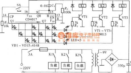
The picture shows the multi-channel multi-state control switch composed of CD4017. The circuit uses a single button control and is controled by eight count output terminals Q1-Q7 through AND GATE circuit composed of diode matrix. Then the three groups of controlled circuits will have eight kinds of working states which will have some practical value in some cases. (View)
View full Circuit Diagram | Comments | Reading(787)
Alternating Current Voltage Multiplier(MC1594) Circuit
Published:2011/7/21 6:54:00 Author:Sue | Keyword: Alternating Current, Voltage, Multiplier
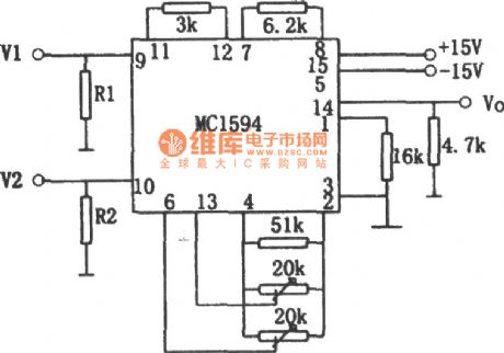
The picture shows the alternating current voltage multiplier circuit. The circuit is composed of MC1594 four-quadrant multiplier .It is very simple but is not very precised. In order to make the circuit work in linearization range, the resistance value of the input terminal's resistor R1 and R2 will be decided by input voltage. R1= V1×6. R2=V2×3. If V1=V2=3V, then R1=18kΩ, R2=9kΩ. When there are different input voltages, R1=52kΩ, R2=30kΩ. But this will slow down the precision and degree of linearity. The relation between the input and output is: Vo=V1V2/10. (View)
View full Circuit Diagram | Comments | Reading(1061)
Multifunctional Adjustable Generalized Time Relay(NE555,CD4013) Circuit
Published:2011/7/23 6:06:00 Author:Sue | Keyword: Multifunctional, Adjustable, Generalized Time Relay
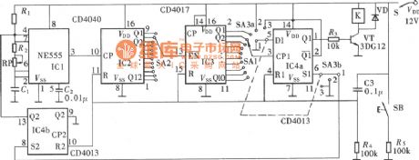
The circuit's multifunction means that it can acheive the three working modes conversions of delayed connection , delayed release , delayed loop . Delayed connection means that after the relay is preset, the relay isn't connected. Only when it reaches the preset timing time can it be connected. Delayed release is just the opposite to delayed connection. After the preset, the relay is connected. When it reaches the preset timing time, the relay is released. The operations of the two working modes of delayed connection and delayed release are one-time. When the relay completes one working process, the circuit's control part will enter into a stable state. (View)
View full Circuit Diagram | Comments | Reading(1189)
RC-π Type Filter Circuit
Published:2011/7/20 20:39:00 Author:Sue | Keyword: Filter
The figure shows RC-π type filter circuit. (View)
View full Circuit Diagram | Comments | Reading(797)
Multiplying Circuit 3(LM101A,HA2-2520)
Published:2011/7/22 5:38:00 Author:Sue | Keyword: Multiplying Circuit
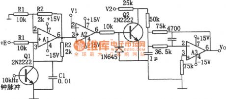
The picture shows the multiplying circuit. A1 composes voltage-control current source. A2 composes voltage comparator. A3 composes active low pass filter. When the time constant R1C1 is equal to the clock pulse period, the relation between the input and output is: Vo=-V1V2/E. If E =1V, then Vo=-V1V2. V1,V2 are required to be positive and should be limited within 10V. V1 should be slightly lower than E. The resistor R1,R2 and capacitor C1 are required to use components with good temperature stability. A1 is HA2-2520. A2,A3 is LM101A. (View)
View full Circuit Diagram | Comments | Reading(732)
Touch Power Supply Switch Circuit Composed of CD4013
Published:2011/7/20 20:30:00 Author:Sue | Keyword: Touch, Power Supply, Switch
As seen in the figure, CD4013 can compose touch switch, which can be connected by being touched once. Another touch can make it disconnected. (View)
View full Circuit Diagram | Comments | Reading(2777)
Temperature controller 6
Published:2011/7/25 21:45:00 Author:Ecco | Keyword: Temperature controller
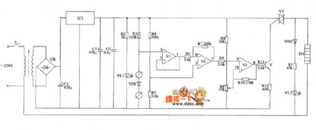
The temperature controller circuit is composed of the power supply circuit, temperature detection control circuit and control implementation circuit, and it is shown as the chart. Power supply circuit is composed of the power switch S, power transformer T, bridge rectifier UR, filter capacitors Cl ~ C3, three-terminal voltage regulator integrated circuit IC1, resistor R2 and power indicator LED YL1. Temperature detection control circuit is composed of the temperature detection diode VD1, resistors R3 ~ R1O, operational amplifier integrated circuit IC2 (N1 ~ N3) and the potentiometer RP. Control implementation circuit is composed of the resistors R11, R12, transistor V and thyristor VT.
(View)
View full Circuit Diagram | Comments | Reading(591)
Temperature controller 7
Published:2011/7/25 21:49:00 Author:Ecco | Keyword: Temperature controller
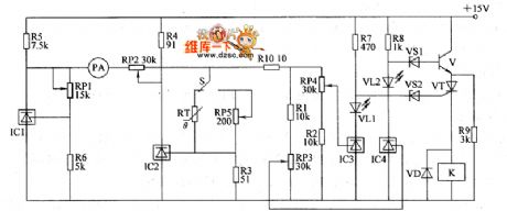
The temperature controller circuit is composed of the temperature detection circuit and temperature control circuit, and it is shown as the chart. Temperature detection circuit is composed of the temperature sensor (thermistor) RT, three-terminal precision regulators ICl, IC2, potentiometers RP1, RP2, RP5, ammeter (temperature indication with) PA, resistors R3 ~ R5 and temperature measurement / set switch. Temperature control circuit consists of three-terminal precision regulators IC3, IC4, transistor V, thyristor VT, voltage regulator diodes VS1, VS2, relay K, diode VD, LEDs VL1, VL2, resistors RI, R2, R7 ~ RIO and temperature UCL potentiometers RP3, RP4, temperature LC potentiometer.
(View)
View full Circuit Diagram | Comments | Reading(599)
| Pages:190/312 At 20181182183184185186187188189190191192193194195196197198199200Under 20 |
Circuit Categories
power supply circuit
Amplifier Circuit
Basic Circuit
LED and Light Circuit
Sensor Circuit
Signal Processing
Electrical Equipment Circuit
Control Circuit
Remote Control Circuit
A/D-D/A Converter Circuit
Audio Circuit
Measuring and Test Circuit
Communication Circuit
Computer-Related Circuit
555 Circuit
Automotive Circuit
Repairing Circuit