
Index 182
12_kW_144_MHz_AMPLIFIER_CONTROL_CIRCUITRY
Published:2009/6/18 2:06:00 Author:May
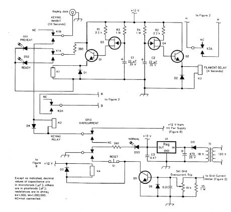
Schematic diagram of the amplifier-control circuits. (View)
View full Circuit Diagram | Comments | Reading(572)
HORN_CIRCUIT_FOR_MOTORCYCLE_USE
Published:2009/6/18 2:02:00 Author:May
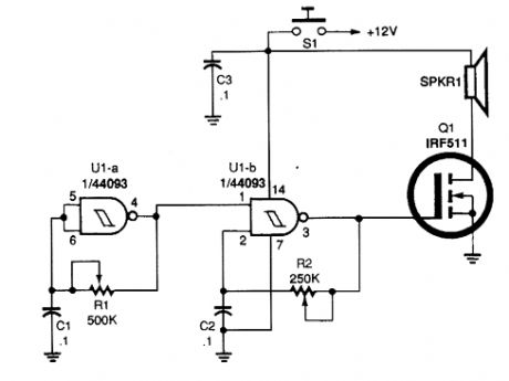
Gates U1-a and U1-b of the 4093 quad 2-tnput NAND Schmitt trigger are connected in variable, low-frequency, square-wave oscillator circuits. The output of gate U1-a is connected to one of the inputs of gate U1-b. The square-wave output of gate U1-a modulates oscillator U1-b, producing a two-tone output. A really interesting sound can be producecl by carefully adjusting po-tentiometers R1 and R2. (View)
View full Circuit Diagram | Comments | Reading(3648)
MOTORCYCLE_BURGLAR_ALARM
Published:2009/6/18 2:00:00 Author:May
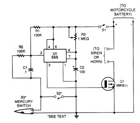
A 555 IC is connected in a one-shot timer cir-cuit that turns on a FET transistor and either a siren or the bike's horn for a preset time period. Switch S1 is used as an on/off switch.Closing either of two switches, S2 and S3, will trigger the IC. When either switch closes, pin 2 of UI goes low. That triggers the IC to produce a positive output at pin 3 and sounds the alarm for the time period set by R3. The mercury switch, S3, is the switch that activates the alarm should anyone move your bike. Switch S2 can be used as a panic switch. (View)
View full Circuit Diagram | Comments | Reading(0)
DOOR_AJAR_INDIGATOR
Published:2009/6/18 1:58:00 Author:May
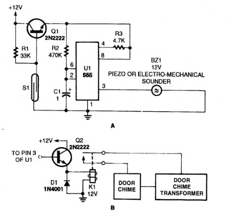
This simple sounder (AJ makes a good door annunciator. If the buzzer is replaced with the circuit in B, the annunciator can be made more pleasant to the ear.
(View)
View full Circuit Diagram | Comments | Reading(1060)
SIMPLE_BIKE_HORN
Published:2009/6/18 1:57:00 Author:May
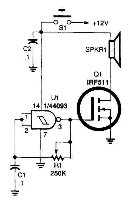
The horn circuit uses only one gate of a 4093 quad 2-input NAND Schmitt trigger, U1, con-nected in a simple, low-frequency, square-wave oscillator circuit. The oscillator's output, at pin 3, drives the gate of Q1. The drain of that FET drives a small horn speaker.Potentiometer RI can be adjusted to set the horn's output frequency. Some horn speakers are frequency sensitive, so play with the oscillator's frequency control for the best or loudest sound. (View)
View full Circuit Diagram | Comments | Reading(2064)
MOTORCYCLE_ALARM
Published:2009/6/17 23:34:00 Author:May
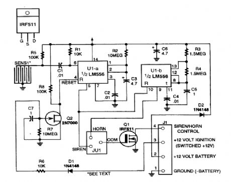
A dual tinter is used to generate a long pulse, which gates a second timer, producing a square wave (nonsymmetrical) and controls the on/off time of the hom. Siren operation can be selected with a jumper. In this case, the output of Q1 will be continuously on and not cycled. Sensor S1 is a row of adjacent circuit board traces with a stainless steel ball bearing laying on them. Any movement causes momentary shorting and opening of the circuit, triggering U1-a. (View)
View full Circuit Diagram | Comments | Reading(155)
CAR_ALARM_DECOY
Published:2009/6/17 23:32:00 Author:May
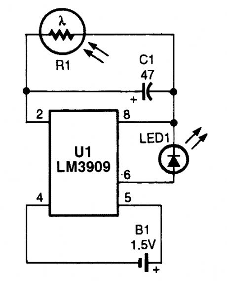
The device will simulate the presence of a burglar alarm in automobiles or homes. Mount RI where daylight can fall on it. During darkness, LED1 flashes, making potential intruders think an alarm system is installed. (View)
View full Circuit Diagram | Comments | Reading(910)
BURGLAR_ALARM_CIRCUIT
Published:2009/6/17 23:18:00 Author:May
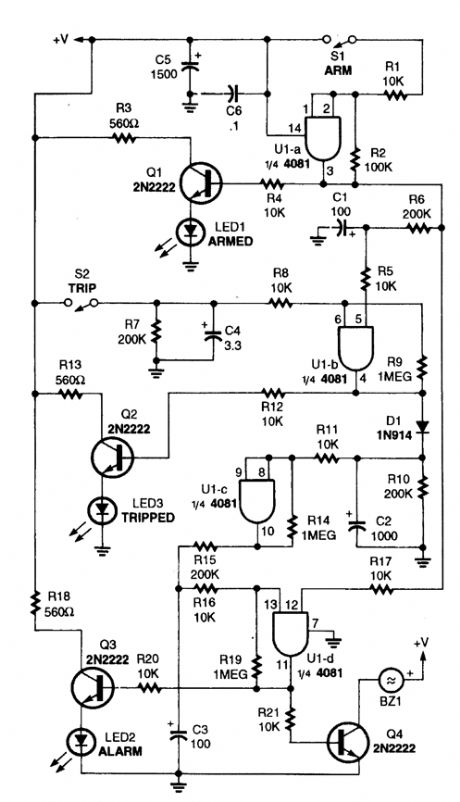
This alarm circuit is built around a single 4081 (CMOS) quad AND gate. It offers an exit and entry delay (around automatically reset two minutes after tripping, provided that the trip input is not left high).The arming switch must go high to arm or low to disarm. After arming, U1-a begins to charge C1 via R6. Around 20 seconds later (af-ter the exit delay), C1 has a sufficient charge to produce a high at the pin-5 input of UI-b.Also, when the circuit is armed, Q1 is turned on to indicate arming, and one input of U1-d is brought high.After the exit delay times out, if the trip in-put opens, it causes an output on gate U1-b.Transistor Q1 is turned on, lighting the trip indi-cator (LED3), C2 instantly charges, and the out-put of U1-c goes high. At that point, C3 begins charging to provide the entry delay.After 20 seconds, C3 has sufficient charge to produce a high at pin 13 of UI -d. That forces UI-d's output high, tuning Q3 and Q4 on, which activates the alarm indicator (LED2) and sounder (BZ1), respectively. If disarmed after a trip pulse, but before the 20-second, entry delay time out, pin 12 of U1-d goes low, so the gate's output does not go high and the alarm does not sound.Components C2 and RIO hold U1-c on for around 2 minutes and 20 seconds to provide the two-minute alarm. After C2's charge drops below half of the supply voltage, U1-c's output goes low, awaiting another trip pulse to set it off again. (View)
View full Circuit Diagram | Comments | Reading(0)
AUDIO_LEVELER
Published:2009/6/17 22:56:00 Author:May
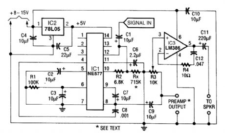
A low power programmable compandor chip, the Signetics NE577IC is used. Incoming audio is compressed, rectified and conditioned so that the input signal level always remains about the noise level. The compressor is an ALC circuit that outputs a constant level and the expander part of the IC is not used. (View)
View full Circuit Diagram | Comments | Reading(2846)
IF_AGO_NETWORK
Published:2009/6/17 22:56:00 Author:May
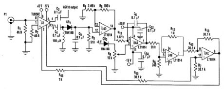
A simple IF AGC circuit that features wide dynamic range and excellent linearity can be achieved with two chips: Tl's TL026C voltage-controlled amplifier IC and Linear Technology's LT1014 (or any other similar basic quad op amp).
(View)
View full Circuit Diagram | Comments | Reading(1768)
3_MHz_LOW_NOISE_AGO_SYSTEM
Published:2009/6/17 22:53:00 Author:May
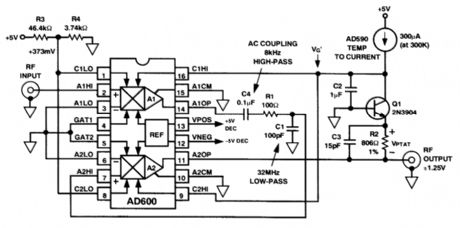
The AD600 dual voltage-controlled amplifier In this circuit provides a 3-MHz AGC system with80-dB range. (View)
View full Circuit Diagram | Comments | Reading(566)
SENSOR_ACTIVATED_RELAY_PULSER
Published:2009/6/17 22:46:00 Author:May
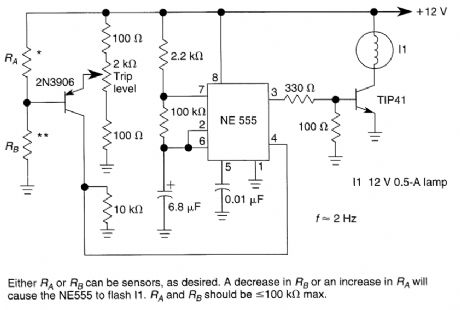
A sensor turns on Q1 to activate the low-frequency 555 oscillator, which pulses LAMP I1. Sensor may be sensitive to changes in light or temperature. (View)
View full Circuit Diagram | Comments | Reading(768)
TIME_DELAY_RELAY_
Published:2009/6/17 22:45:00 Author:May
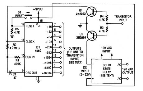
Using a 4060 CMOS binary divider and built-in clock oscillator, a long-duration timer can be made very simply. The solid-state relay can be sized for your application, and can be replaced with a mechanical relay if a suitable power supply is available. With the components shown, a 4.5-Hz clock frequency is generated. Divided outputs are available from÷ 4 to 16384 (about 4 hours). (View)
View full Circuit Diagram | Comments | Reading(4989)
SOLID_STATE_RELAY_CIRCUITS
Published:2009/6/17 22:41:00 Author:May
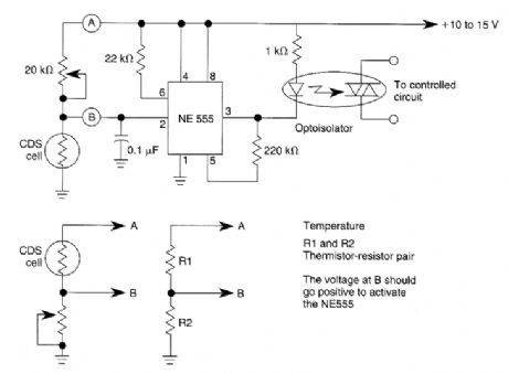
This dark-activated relay switch can be used to turn on walkway or other outdoor lighting at dusk. By using alternate connections to A and B, increasing illumination, high and low temperatures can be sensed. (View)
View full Circuit Diagram | Comments | Reading(1274)
SOLID_STATE_RELAY_CIRCUIT
Published:2009/6/17 22:39:00 Author:May
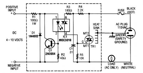
R1 limits input current while Q1 acts as a current sink to protect IC1. D1 serves as a polarity pro-tector. IC1 provides a trihc output to trigger the main triac, TR1. (View)
View full Circuit Diagram | Comments | Reading(2101)
SOLID_STATE_LATCHING_RELAY
Published:2009/6/17 22:38:00 Author:May
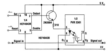
This simple circuit provides a solid-state equivalent of the electromechanical latching relay (see the figure). What's more, the switching is clean, highly resistant to vibration and shock, and isn't sen-sitive to magnetic fields or position.The circuit operates as follows: a set pulse to the 4043 RS latch takes its output high and turn on the 2N3904 transistor. Current will then flow through the photovoltaic relay's LED and the resistance between D1 and D2 will fall from several gigaohms to less than 30 Ω. The PVR will remain in this state until a reset pulse is received by the 4043 RS latch. (View)
View full Circuit Diagram | Comments | Reading(2008)
PROXIMITY_ALARM_II
Published:2009/6/17 21:10:00 Author:May
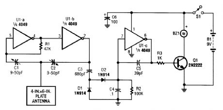
A CMOS logic gate is used to make up this circuit. When an object is near the antenna, the change in oscillator output is detected by D1 and D2 and amplified by U1C, which drives Q1, sound-ing alarm BZ1. (View)
View full Circuit Diagram | Comments | Reading(874)
PROXIMITY_ALARM_I
Published:2009/6/17 21:08:00 Author:May
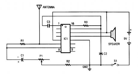
IC1 contains several oscillators and an amplifier. The low-frequency audio-signal oscillator is used to supply an input to the amplifier. That signal is the audio tone that is amplified, then supplied to the speaker by the amplifier.The high-frequency oscillator is purposely set to be very unstable. It is dormant or off until the resistor-capacitor (RC) network is changed. The resistance (fi) in this case is made up of R2 and P1. As the resistance of Pl is decreased, the unit becomes more sensitive (more unstable), and less ca-pacitance (C) is needed to cause the oscillator to oscillate.The capacitance required is provided by C2 and by any capacitance introduced via the antenna loop. When you come near that loop, your inherent body capacitance causes the high-frequency os-cillator to begin to oscillate, which then causes the low-frequency oscillator to be switched on in-ternally. Once the alarm is sounding, the IC is designed so that it latches , that is, it stays on until the power to it is switched off.C1 1-pFAxialCapacitorC2 27-pF Silver Mica CapacitorC3 0.1-pF Mylar CapacitorIC1 CM1001N ICP1 50-kQ Trimmer ResistorR1 75-kQ ResistorR2 200-Q ResistorR3 100-kQ ResistorS1 SPDT SwitchSpk Small SpeakerMisc IC Socket, Battery Snap, Ground Plate, Wire, PC Board (View)
View full Circuit Diagram | Comments | Reading(826)
SIMPLE_SAFETY_CIRCUIT
Published:2009/6/17 21:05:00 Author:May
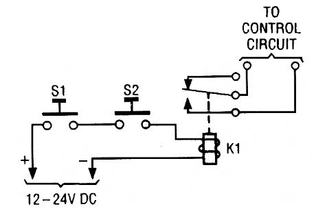
The simple two-hand safety-control switch shown here is little more than two pushbutton switches connected in series; both must be de-pressed in order to energize the relay. (View)
View full Circuit Diagram | Comments | Reading(1048)
LOUDSPEAKER_PROTECTOR
Published:2009/6/17 21:04:00 Author:May
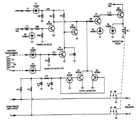
Transistors Q1, Q2, and Q3 monitor the two outputs of the stereo amplifier. If the offsets exceed ±2 V, Q7 is turned off, which turns off Q8 and the normally on relay. Diodes D2 and D5, together vith Q4, provide a mains voltage monitor. As soon as the ac input voltage disappears, as when the ampli-fier is turned off, Q4 turns off and Q5 turns on. This turns off Q7, Q8, and the relay. Hence, the loud-speakers are disconnected immediately after the amplifier is turned off. (View)
View full Circuit Diagram | Comments | Reading(904)
| Pages:182/312 At 20181182183184185186187188189190191192193194195196197198199200Under 20 |
Circuit Categories
power supply circuit
Amplifier Circuit
Basic Circuit
LED and Light Circuit
Sensor Circuit
Signal Processing
Electrical Equipment Circuit
Control Circuit
Remote Control Circuit
A/D-D/A Converter Circuit
Audio Circuit
Measuring and Test Circuit
Communication Circuit
Computer-Related Circuit
555 Circuit
Automotive Circuit
Repairing Circuit