
Index 185
REMOTE_CONTROL_ANALYZER
Published:2009/6/16 22:05:00 Author:May
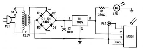
A schematic diagram for the remote analyzer is shown. The circuit is powered from a simple 5-V supply, consisting of PL1, 51, T1, abridge rectifier (comprised of Dl through D4), capacitor C1, and a common 5-V regulator, UI. Switch 51 is the on/off control and is optional. The power-supply trans-former used in the prototype is a 12.6-Vac unit, but any transformer that can supply at least 5.6-Vac will do. The 12.6-V unit was used solely because of its availability.The output of T1 is full-wave rectified by diodes Dl through D4 and filtered by C1. The bumpy dc output from the capacitor is regulated down to 5 V by UI, a 7805 integrated regulator, LED1 acts as a power indicator to let you know that the circuit is active.The 5-Vdc powers a GPIU52X infrared-detector module* (MODl), which demodulates the 40-kHz carrier used by most infrared remotes. After demodulation, the resulting logic pulses are sent to an oscilloscope via PL2, a BNC connector.
*Radio Shack part #276-137 (View)
View full Circuit Diagram | Comments | Reading(1006)
GEIGER_COUNTER_Ⅱ
Published:2009/6/16 21:56:00 Author:May
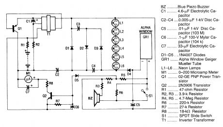
BZ..........Blue Piezo Buzzerc1......... 4.6-ptF Electrolytic CapacitorC2-04....0.005-μF 1-kV Disc CapacitorC5..........01-μF 1-kV Dtsc Capacitor (103 M)CG..........1-μF 100-V Mylar Capacitor (104 k)07......... 33-p.F Electrolytic CapacitorD1-D5....1N4007 DiodesGR1....... Alpha Window Geiger MuellerTubeL1-L6......Neon LampsM1......... 0-200 Microamp Meter Q1......... 02-GE PNP Power TransistorQ2......... 2N39O6 TransistorR1......... .7-ohm ReststorR2, R3,.. .3.9-k ResistorR4, R5.... 4.7-Meg ResistorR6......... 220-k ResistorR7......... .27-k ResistorR8.....,....18-kf) Resistor51.......... SPDT Slide SwitchT1......... InverterTransformer
Q1 is a pnp power transistor used in conjunction with a ferrite transformer to form a blocking-type oscillator. This oscillator is a fixed-frequency type, and the feedback to sustain oscillations is from capacitor C1. Because of the turns ratio of T1, the small ac voltage produced on its primary is converted to a large ac voltage on its secondary. That high-voltage ac is applied to the voltage trip-per stage, which consists of capacitors C2, C3, and C4 and diodes D1, D2, and D3. The resultant volt-age is now over 800 V and it is regulated by neon lamps L1 through L6. Diode D4 rectifies the high voltage and applies it to the cathode lead of the GM tube. The positive (+) bias on the GM tube is ap-plied to the anode by way of load resistors R4 and R5. Each time a radioactive particle strikes the GM tube, it causes the gas inside to ionize. This ionization of the gas creates a pulse, which drives the piezo speaker and is also coupled by diode D5 to the base of Q2. Transistor Q2 is a pnp type and is used to integrate the pulses in conjunction with capacitor C6. That produces a dc voltage level, which is in proportion to the quantity of pulses arriving at the base of Q2. The collector of Q2 is con-nected through resistor R8 to the (+) terminal of the meter. The other side of the meter goes directly to (-) of the battery. (View)
View full Circuit Diagram | Comments | Reading(2057)
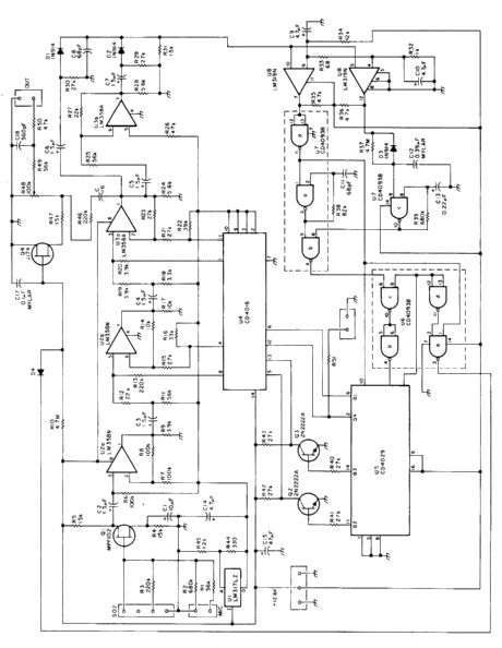
GEIGER_COUNTER_I
Published:2009/6/16 21:51:00 Author:May
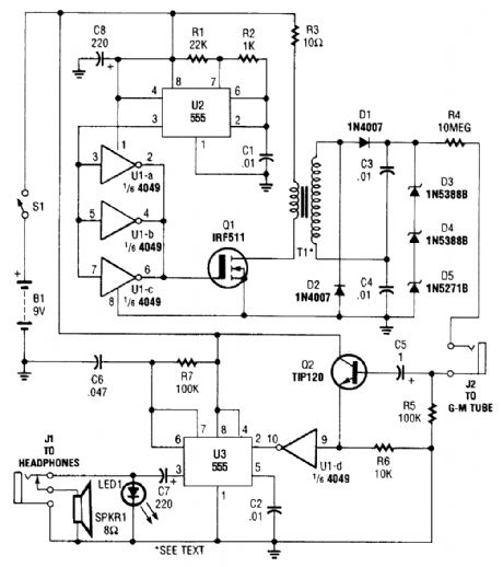
The circuit is built around a 4049 hex inverter (U1), a pair of 555 oscillator/timers (U2 and U3), two transistors, a Geiger-Muller tube, and a few additional support components. The first 555 (U2) is configured for astable operation. The output of U2 (a series of negative-going pulses) at pin 3 is fed to three parallel-connected inverters (U1-a, U1-b, and U1-c). The positive-going output pulses of the inverters are fed to the gate of Q1, causing it to toggle on and off.The output of Q1, which is connected in series with the primary of step-up transformer T1, pro-cluces a stepped-up series of pulses in T1's secondary. The output of T1 (approximately 300 V) is fed through a voltage doubler (consisting of D1, D2, C3, and C4), producing a voltage of around 600 V Three series-connected Zener diodes (D3, D4, and D5) are placed across the output of the voltage dou-bler to regulate the output to 500 V, fed through R4 (a 10-MΩ current-limiting resistor) and J2 to the anode of the GM tube. The limiting resistor also allows the detection ionization to be quenched.The cathode side of the tube is connected to ground through a 100-kΩ resistor, R5. When a par-ticle is detected by the GM tube, the gases within the tube ionize, producing a pulse across R5. That pulse is also fed through C5 and applied to the base of Q2 (a TIP120 npn transistor), where it is am-plified and clamped to 9V. The output of Q2 is inverted by gate U1-d, then it is used to trigger U3 (the second 555, which is configured for monostable operation). The output of U3 at pin 3 causes LED1 to flash, and produces a click that can be heard through speaker SPKR1 or headphones. The circuit is powered by a 9-V alkaline battery and draws about 28 mA when not detecting radiation. (View)
View full Circuit Diagram | Comments | Reading(1799)
HEADLIGHT_ALARM
Published:2009/6/16 3:01:00 Author:May
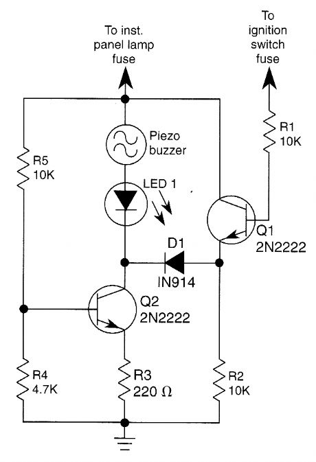
The base of Q1 is connected to the car's ignition circuit; the easiest point to make that connection is at the ignition switch fuse in the car's fuse panel. Also, one side of the piezoelectric buzzer is connected to the instrument-panel light fuse; when the headlights or parking lights are on, the instrument panel is lit, too. When the headlights are off, no current reaches the buzzer. Therefore, nothing happens. What happens when the head-lights are on depends on the state of the ignition switch. When the ignition switch is on, transistors Q1 and Q2 are biased on, effectively removing the buzzer and the LED from the circuit.When the ignition switch is turned off, but the headlight switch remains on, transistor Q1 is turned off, but transistor Q2 continues to be biased on. The result is that the voltage across the piezoelectric buzzer and the LED is sufficient to cause the buzzer to sound loudly and the LED to light. (View)
View full Circuit Diagram | Comments | Reading(386)
LAMP_SWITCHING_CIRCUIT
Published:2009/6/16 2:49:00 Author:May
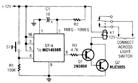
A normally open pushbutton switch (51) delivers a positive input pulse to pin 4 of U1, triggering the IC into action. The output of U1 at pin 6 supplies base-drive current to a Darlington pair comprised of Q1 and Q2, activating K1. A 10-μF capacitor and any resistor value of from 1 to 10 MΩ can be used as the timing components.To use the circuit on an auto's headlights, connect the relay's normally open contacts across the car's headlight switch and press S1 to extend the on time. In connecting the circuit to control an acoperated lamp, turn off the ac power and connect the relay contacts in parallel with the lamp's power switch contacts. (View)
View full Circuit Diagram | Comments | Reading(895)
AUTO_TURN_SIGNAL_REMINDER
Published:2009/6/16 2:35:00 Author:May
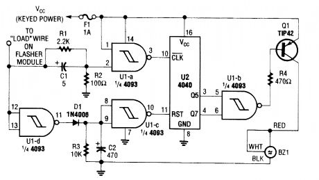
This circuit counts turn signal flashes. At the end of about 70 flashes, a chime sounds to remind the driver to turn off the turn signal. By using various taps on U2, the period can be changed if de-sired. BZ1 is a buzzer or chime module. (View)
View full Circuit Diagram | Comments | Reading(971)
TIME_DELAY_AUTO_KILL_SEITCH
Published:2009/6/16 2:29:00 Author:May
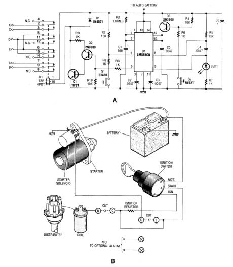
The automobile delayed kill switch is simple in concept. When you get out of your car, a secretly located pushbutton switch is pressed. Nothing apparently happens, but at the end of a predeter-mined time, a relay is pulled in and locked. When the relay is pulled in, contacts open, and the hot lead from the ignition to the coil and the hot wire from the key switch to the starter solenoid is opened or disconnected. If the engine is running, it stops immediately and the starter will not operate. When you get into the car, another pushbutton switch is pressed and the relay drops out and everything goes back to normal. (View)
View full Circuit Diagram | Comments | Reading(1334)
REMOTE_FIELD_STRENGTH_METER
Published:2009/6/16 2:10:00 Author:May
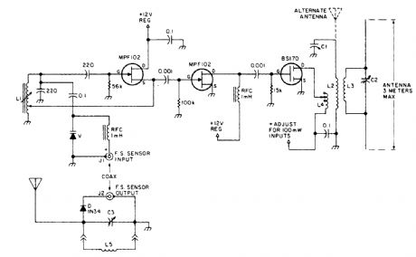
This field strength meter consists of a tuned crystal detector producing a dc output voltage from a transmitted signal. The dc voltage is used to shift the frequency of a transmitter of 100-mW power operating at 1650 kHz. The frequency shift is proportional to the received field strength. This unit has a range of several hundred feet and is operated under FCC part 15 rules (100-mW max power into a 2-m-long antenna between 510 and 1705 kHz). (View)
View full Circuit Diagram | Comments | Reading(779)
ELECTRONIC_DOOR_BUZZER
Published:2009/6/16 2:00:00 Author:May
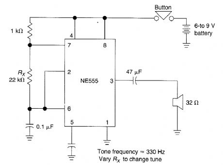
This simple electronic door buzzer draws no quiescent current. When S1 is pressed the speaker produces a tone. The NE555 (U1) generates signal. (View)
View full Circuit Diagram | Comments | Reading(3)
TWIN_BELL_CIRCUIT
Published:2009/6/16 1:59:00 Author:May
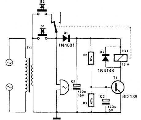
It is often desirable for a single doorbell to be operated by two buttons, for instance, one at the front door and the other at the back door.The additional button, S2 in series with the break contact of relay Re 1, is connected in parallel with Lhe original bell-push, S1. When S2 is pressed, the bell voltage is rectified by D1 and smoothed by Cl. After a time, t= R1R2C2, the direct voltage across C2 has risen to a level here T1 switches on. Relay Rel is then energized and its contact breaks the circuit of S2 so that the bell stops ringing. After a short time, C1 and C2 are discharged, the relay retums to its quiescent state and the bell rings again.In this way, S1 will cause the bell to ring continuously, while S2 makes it ring in short bursts, so that it is immediately clear which button is pushed. (View)
View full Circuit Diagram | Comments | Reading(884)
ELECTRONIC_DOORBEL
Published:2009/6/16 1:56:00 Author:May
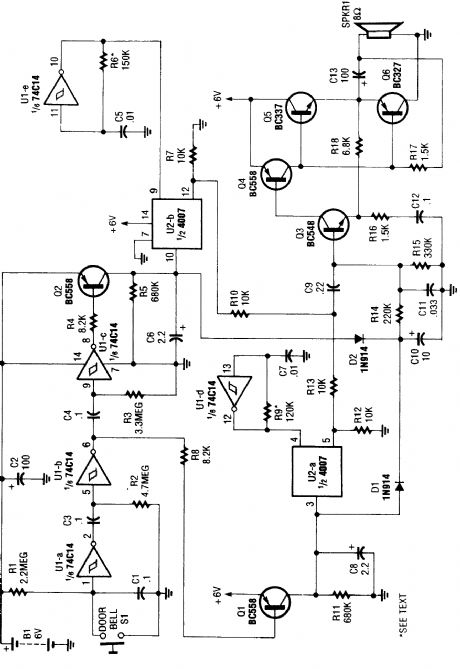
When the doorbell switch is pressed,the two monostable stages are activated in sequence,appling bias to a pair of voltagecontrolled resistor stages.These then modulate the outputs fro, a pair of tone generators.The resulting signals are fed to an audio amplifier,then to the speaker. (View)
View full Circuit Diagram | Comments | Reading(801)
ALCAUTOMATIC_LEVEL_CONTROL
Published:2009/6/15 23:33:00 Author:May
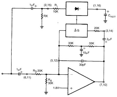
The rectifier input is tied to the input. This makes gain inversely proportional to input level so that a 20-dB drop in input level will produce a 20-dB increase in gain. The output will remain fixed at a constant level. The circuit will main-tain an output level of ±1 dB for an input range of +14 to -43 dB at 1 kHz. Additional extemal components will allow the output level to be ad-justed. (View)
View full Circuit Diagram | Comments | Reading(592)
DIGITAL_AUTOMATIC_LEVEL_COMTROLALC
Published:2009/6/15 23:26:00 Author:May


This approach to automatic level control(ALC) make use of digitally seitched audio attenuators in the signal path. The out-put level of the system is sensed, compared to a reference, and audio pads are inserted via analog switches. This method is nearly instantaneous and eliminates the compromises necessary in conventional RC network ALC systems useing fast attack,slow-decay approaches. (View)
View full Circuit Diagram | Comments | Reading(1216)
AUDIO_VOLUME_LIMITER
Published:2009/6/15 23:12:00 Author:May
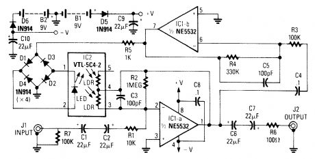
IC1-a is connected as an inverting amplifier whose gain is controlled by the LDR portion of an op-tocoupler. (View)
View full Circuit Diagram | Comments | Reading(2303)
BCD_ROTARY_SWITCH
Published:2009/6/15 23:11:00 Author:May
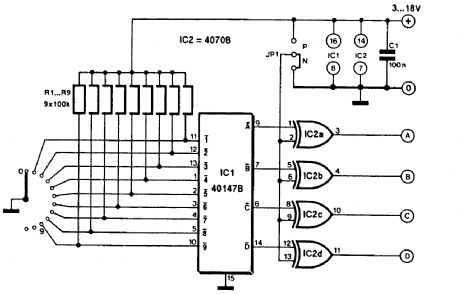
This circuit allows a simple rotary switch to emulate a BCD switch. The circuit draws about 200 mA. A 10-position rotary switch is used. (View)
View full Circuit Diagram | Comments | Reading(5004)
DIGITAL_CAPACITANCE_CONTROL
Published:2009/6/15 23:09:00 Author:May
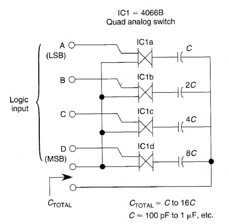
Digital capacitance control is possible with bilateral switches. Do not forget to consider ON resistance of the analog switches. (View)
View full Circuit Diagram | Comments | Reading(661)
DIGITAL_RESISTANCE_CONTROL
Published:2009/6/15 23:09:00 Author:May

Digital resistance control is possible with bilateral switches. Do not forget that analog switches have on resistance. (View)
View full Circuit Diagram | Comments | Reading(1103)
DIGITAL_MULTIPLE_GANG_POTENTIOMETER_CONTROL
Published:2009/6/15 23:06:00 Author:May
A 555 timer can be configured to simulate a multi-gang potentiometer by controlling the markspace ratio. The switching rate should be at least twice the maximum expected signal frequency the potentiometer has to handle. (View)
View full Circuit Diagram | Comments | Reading(744)
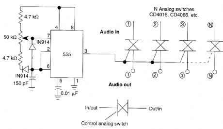
DIGITAL_AUDIO_SELECTOR
Published:2009/6/15 23:05:00 Author:May
This circuit uses switched emitter followers, rather than the usual analog switch CMOS chips. This yields better reduction of crosstalk between channels. This circuit can handle up to 4 Vrms with less than -80-dB crosstalk. (View)
View full Circuit Diagram | Comments | Reading(1512)
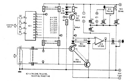
DIGITAL_ENTRY_LOCk
Published:2009/6/15 23:00:00 Author:May

A block pinout diagram of the LS7220 keyless-lock IC is shown. The keypad must provide each key with a contact to a common connection. In this case, the common connection goes to the posi-tive supply rail so that when a key is pressed, a positive voltage is passed through to the wire associ-ated with that key. Each of the 12 keys are brought out to separate wires, and each wire is connected to a different pin of a 24-pin socket (SO1).To activate (unlock) the circuit, a preprogrammed four-digit access code must be entered in the proper sequence. The four-digit access code must be entered in the proper sequence. The four-digit access is programmed into the' circuit by connecting jumpers between terrrtinals of a 24-pin plug-in header.When the correct access code is entered (in the proper sequence), positive voltages appear at pins 3, 4, 5, and 6 of U1. That causes U1 to output a positive voltage at pin 13, which is fed through resistor R2 to the base of Q1, causing it to conduct. With Q1 conducting, its collector is pulled to ground potential, energizing relay K1. The normally open relay contacts close, switching on any ex-ternal device.Capacitor C2 controls the total time that the output of U1 at pin 13 is positive after the release of the first key. With avalue of 3.3 pF for C2, active time after release of the first key is about two sec-onds, assuming a 6-V supply or four seconds with a 12-V supply. Therefore, if you push the subse-quent keys too slowly, the relay might not close at all! To increase the time allotted for code entry, you will have to increase the capacitance of C2. (View)
View full Circuit Diagram | Comments | Reading(2)
| Pages:185/312 At 20181182183184185186187188189190191192193194195196197198199200Under 20 |
Circuit Categories
power supply circuit
Amplifier Circuit
Basic Circuit
LED and Light Circuit
Sensor Circuit
Signal Processing
Electrical Equipment Circuit
Control Circuit
Remote Control Circuit
A/D-D/A Converter Circuit
Audio Circuit
Measuring and Test Circuit
Communication Circuit
Computer-Related Circuit
555 Circuit
Automotive Circuit
Repairing Circuit