
Circuit Diagram
Index 1039
1_1000_GAIN_RANGE
Published:2009/7/6 6:39:00 Author:May
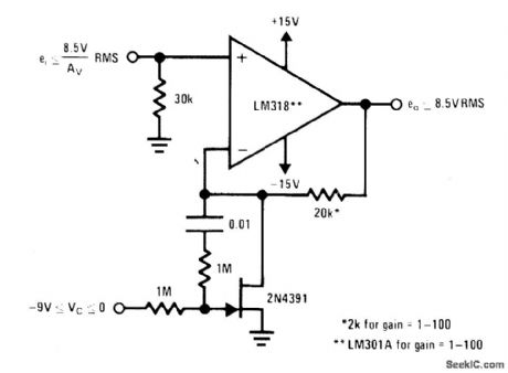

Control voltage of 0 to -9 V changes gain of amplifier over complete range while providing maximum output level of 8.5 VRMS and bandwidth of over 20 kHz at maximum gain. If gain range of 100 is sufficient, amplifier can be changed to LM30lA; 20K resistor is then changed to 2K.- Linear Applications, Vol. 2, National Semiconductor, Santa Clara, CA, 1976, AN-129, p 5. (View)
View full Circuit Diagram | Comments | Reading(846)
LOW_TEMPERATURE_COEFFICIENT
Published:2009/7/6 6:36:00 Author:May
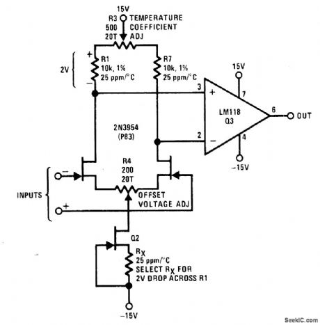
Use of National 2N3954 dual FET as input device for opamp gives fast response to thermal transients, making it possible to adjust R3 and R4 so temperature coefficient is less than 5 μV/℃ from -25℃ to +85℃. Common-mode rejection ratio is typically greater than 100 dB for input voltage swings of 5 V, Drain current level is set by Q2 which is 2N5457 FET.- FET Databook, National Semieonductor, Santa Clara, CA, 1977, p 6-4-6-7. (View)
View full Circuit Diagram | Comments | Reading(1416)
POSTAMPLIFIER
Published:2009/7/6 6:35:00 Author:May
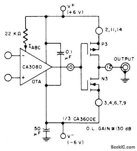
CMOS transistor pall fromCA3600E transistor array provides additional 30-dB gain above 100-dB gain of CA3080 opamp to give total of 130 dB. Current output is about10 mA. Remaining transistor pairs of array can be paralleled pail shown to give greater output. – Linear Integrated Circuits and MOS/FET's, RCA Solid State Division, Somerville, NJ, 1977, p 278-279. (View)
View full Circuit Diagram | Comments | Reading(858)
ARMATURE_TESTING_BRIDGE
Published:2009/7/22 22:55:00 Author:Jessie

Identical current pulses are injected into perfect standard armature and production armature being tested. Transient response, displayed on cro, permits fault diagnosis and location. Choice of four operating modes provides operating flexibility.-H. R. Weed and S. K. Weed, Pulse Response Pinpoints Armature Foults, Electronics, 33:24, p 70-72. (View)
View full Circuit Diagram | Comments | Reading(802)
100_kHz_BUFFERED_RECTIFIER
Published:2009/7/6 6:34:00 Author:May
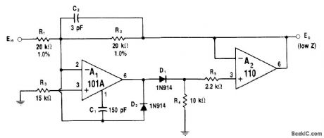
High-speed 110 voltage follower is used within feedback loop of A1 to maintain low output impedance for precision half-wave rectifier, When input signal is positive, D1 and R4 rectify signal and A2 follows this signal. On opposite alternations, D1 is off and feedback loop of A2 is closed through D2 so output terminal is maintained at low impedance. For opposite output polarity, reverse diode connections.-W. G. Jung, IC Op-Amp Cookbook, Howard W. Sams, Indianapolis, IN, 1974, p 192. (View)
View full Circuit Diagram | Comments | Reading(995)
TRANSISTOR_TESTER_WITH_SPEAKER
Published:2009/7/22 22:53:00 Author:Jessie
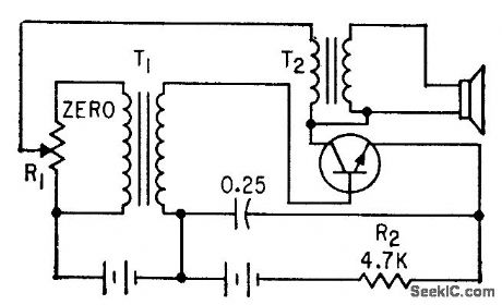
Blocking-oscillator test circuit provides tone from speaker only when transistor is good (not open, shorted, or leaky). Runaway transistors con be detected by providing npn-pnp switch and reversing it to stop oscillation for a few seconds, then restoring correct position. If transistor then oscillates al different frequency or will not resume oscillation, it is a runaway.-L. G. Sands, Dynamic Testers For Transistors, Electronics, 33:8, p 66-67. (View)
View full Circuit Diagram | Comments | Reading(836)
POWER_BOOSTER
Published:2009/7/6 6:33:00 Author:May
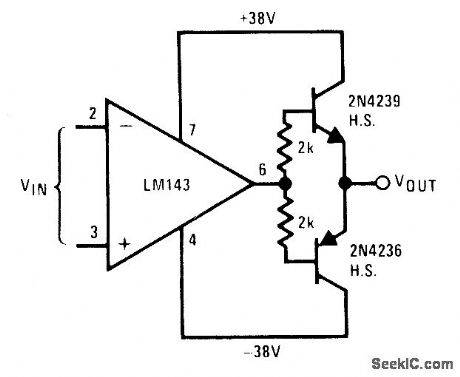
Simple two-transistor power stage increases power output of LM143 high-voltage opamp. Intended for loads less than 2K. Drawbacks are noticeable crossover distortion and lack of short-circuit protection. Transistors should be used with Thermalloy 2230-5 or equivalent heatsinks.- Linear Applications, Vol. 2, National Semiconductor, Santa Clara, CA, 1976, AN-127, p 3. (View)
View full Circuit Diagram | Comments | Reading(2561)
PHASE_ERROR_TESTER
Published:2009/7/6 6:32:00 Author:May
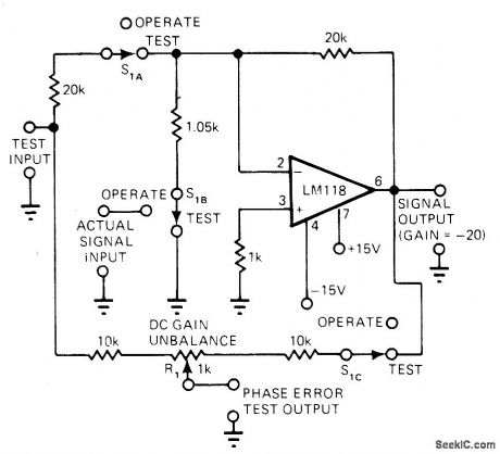
Circuit reveals significant phase errors at relatively low frequencies, even for high-speed opamps. Technique applies to most opamps and almost any signal gain. Article gives operating instructions based on observation of null with XY CRO connected to phase-error test output.-R. A. Pease, Technique Trims Op-Amp Amplifiers for Low Phase Shift, EDN Magazine, Aug. 20, 1977, p 138. (View)
View full Circuit Diagram | Comments | Reading(661)
1_of_15_cascaded_video_mux
Published:2009/7/22 22:53:00 Author:Jessie
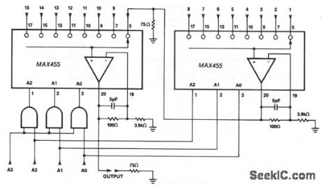
In this circuit, two MAX455s are cascaded to form a 1-of-15 video MUX by connecting the output of one MUX to one input of the input channels of a second MUX. Although the two devices are usually close to one another, the out-put of the first MUX should be terminated to preserve bandwidth.
(View)
View full Circuit Diagram | Comments | Reading(712)
DYNAMIC_TRANSISTOR_TESTER
Published:2009/7/22 22:51:00 Author:Jessie
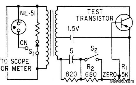
Uses blocking oscillator and depends on fact that open, shorted, or excessively leaky transistors will not oscillate. Good transistors should oscillate with R1 set at zero, and make neon lamp glow if S1 is on.-L. G. Sands, Dynamic rosters For Transistors, Electronics, 33:8, p 66-67. (View)
View full Circuit Diagram | Comments | Reading(1255)
POWER_OPAMP
Published:2009/7/6 6:23:00 Author:May
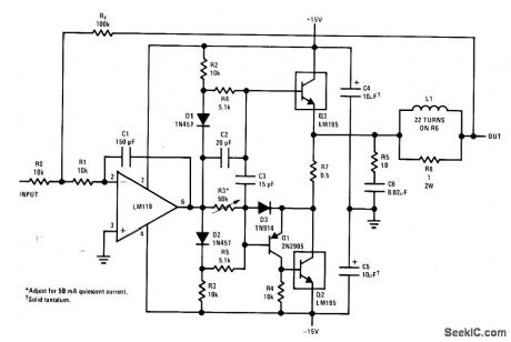
Transistor Q1 and power transistor IC Q2 form equivalent of power PNP transistor for use with NPN LM195 power transistor IC serving as output stage for opamp. Circuit is stable for almost any load. Bandwidth can be increased to 150 kHz with full output response by decreasing C1 to 15 pF if there is no capacitive load to cause oscillation.- Linear Applications, Vol. 2, National Semiconductor, Santa Clara, CA, 1976, AN-110, p 5-6. (View)
View full Circuit Diagram | Comments | Reading(1042)
DIFFERENTIAL_I_O
Published:2009/7/6 6:23:00 Author:May
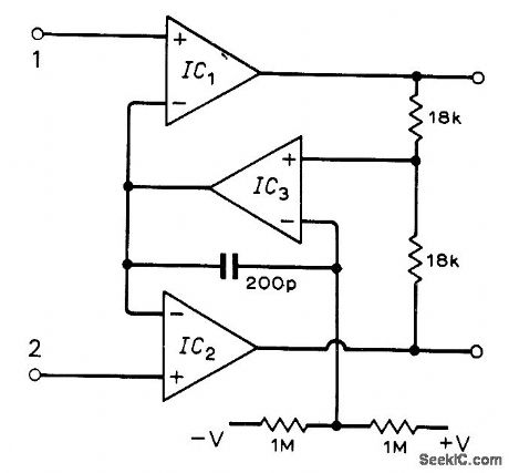
Arrangement shown for three 741 opamps gives amplifier having differential output as well as differential input. Circuit is designed primarily to drive meter with signal of either polarity when center-tap power supply is not available. Article covers operation and adjustment of circuit.-A. D. Monstall, Differential Input and Output with Op-Amps, Wire-less World, Jan. 1973, p 31. (View)
View full Circuit Diagram | Comments | Reading(872)
BOOSTING_VOLTAGE_RATING
Published:2009/7/6 6:22:00 Author:May
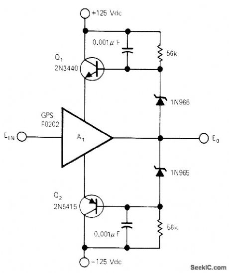
Bootstrapping technique permits operation of low-voltage unity-gain opamp from high-voltage DC supply for handling large input signal voltage swings, while retaining gain and voltage stability of opamp. Allowable input-voltage range depends entirely on transistor rating. With 1000-V transistors, circuit can handle input signals of ±475 V. Input capability for values shown is ±100 V P-P for DC to 10 kHz. Output capability is 5 mA P at t 100 V. Input impedance is 10 teraohms. -S. A. Jensen, High-Voltage Source Follower, EDN IEEE Magazine, Feb. 1, 1972, p 58. (View)
View full Circuit Diagram | Comments | Reading(1765)
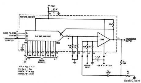
CMOS_A_D_converter_with_positive_true_logicbipolar__VSUBREF_SUB_to___VSUBREF_SUB
Published:2009/7/22 22:50:00 Author:Jessie
This circuit is similar to that of Fig. 6-8, except that the output is positive-true -VREF to + VREF. (View)
View full Circuit Diagram | Comments | Reading(629)
RELAY_CONTACT_CHATTER_TESTER
Published:2009/7/22 22:49:00 Author:Jessie

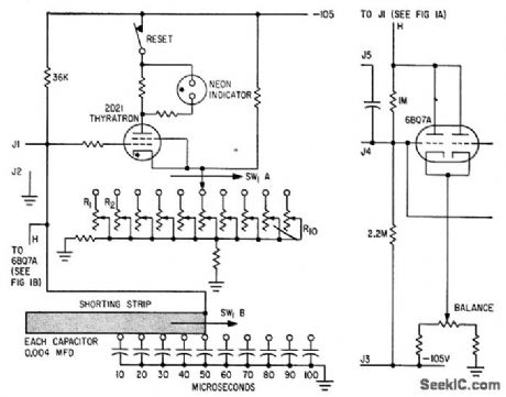
Monitors either open or closed contacts, in 10-microsec increments for intervals of from 10 to 100 microsec. Thyratron conducts if relay contacts remain open (or closed) longer than pre determined interval. Inverter (at right) triggers thyratron during testing of contacts, and is normally open Contacts under test are connected to J3 and J4.-E. H. Kopp, Production Line Checker for Relay Contact Chatter, Electronics, 33:21, p 94-95. (View)
View full Circuit Diagram | Comments | Reading(923)
100_mA_CURRENT_BOOSTER
Published:2009/7/6 6:20:00 Author:May

Provides short-circuit protection along with current boosting for LM143 high-voltage opamp. Diodes are 1N914. Use Thermalloy 2230-5 or equivalent heatsinks, with transistors Output is± 33 V P-P into 400-ohm load.-“Linear Applications, Vol. 2,” National Semiconductor, Santa Clara, CA, 1976, AN-127, p 4. (View)
View full Circuit Diagram | Comments | Reading(2246)
100_kHz_FULL_WAVE_RECTIFIER
Published:2009/7/6 6:19:00 Author:May
Feed-for-ward connection of opamps gives high-speed full-wave rectification of signals up to 100 kHz for measurement and analysis.-W. G. Jung, IC Op-Amp Cookbook, Howard W. Sams, Indianapolis, IN, 1974, p 193-194. (View)
View full Circuit Diagram | Comments | Reading(1256)
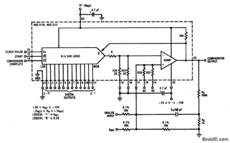
CMOS_A_D_converter_with_positive_true_logic_0_V_to___VSUBREF_SUB_input
Published:2009/7/22 22:47:00 Author:Jessie
This circuit is similar to that of Fig. 6-8, except that the output is positive-true 0 V to + VREF. (View)
View full Circuit Diagram | Comments | Reading(621)
8_channel_video_mux_amplifier
Published:2009/7/22 22:47:00 Author:Jessie
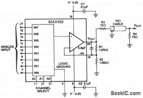
This circuit provides a 50-MHz gain-bandwidth (unity gain at the cable end) video MUX, which is controlled by a 3-wire channel select. The cable is back-terminated (R3) to match cables and reduce reflections. (View)
View full Circuit Diagram | Comments | Reading(739)
MISSING_PULSE_ALARM
Published:2009/7/6 6:15:00 Author:May
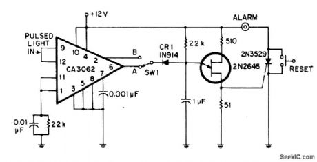
Developed for sensing missing light pulses or detecting absence of object on moving conveyor belt. CA3062 com bination light sensor and amplifier detects light pulses synchronized to 60-Hz line. With SW1 at A, each pulse resets 20-ms timing network of 2N2646 UJT at 16.7-ms intervals, preventing UJT from firing. If light beam is interrupted by object, UJT is allowed to fire and trigger 2N3529 SCR that turns on alarm. With SW1 at B, circuit detects interruptions in steady light beam and sounds alarm only when interruption does not occur.-J. F. Kingsbury, Double Duty Photo Alarm, EDN|EEE Magazine, May 15, 1971, p 51. (View)
View full Circuit Diagram | Comments | Reading(1645)
| Pages:1039/2234 At 2010211022102310241025102610271028102910301031103210331034103510361037103810391040Under 20 |
Circuit Categories
power supply circuit
Amplifier Circuit
Basic Circuit
LED and Light Circuit
Sensor Circuit
Signal Processing
Electrical Equipment Circuit
Control Circuit
Remote Control Circuit
A/D-D/A Converter Circuit
Audio Circuit
Measuring and Test Circuit
Communication Circuit
Computer-Related Circuit
555 Circuit
Automotive Circuit
Repairing Circuit