
Circuit Diagram
Index 2050
Foot blood flowing magnetic buck shoes
Published:2011/4/18 20:07:00 Author:Ecco | Keyword: Foot blood flowing, magnetic , buck shoes

View full Circuit Diagram | Comments | Reading(842)
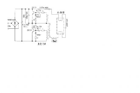
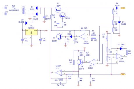
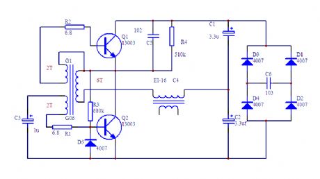
Reliable (15W) switching power supply making circuit diagram
Published:2011/4/20 3:00:00 Author:May | Keyword: 15W, switching power supply
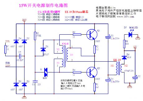
View full Circuit Diagram | Comments | Reading(2791)
Power output stage diagram circuit of switching power supply
Published:2011/4/20 1:21:00 Author:May | Keyword: Power output stage, switching power supply

Power output stage diagram circuit of switching power supply (50KHz-120KHz 1KW-2KW) (View)
View full Circuit Diagram | Comments | Reading(2224)
TDA8132 typical application circuit (switching regualted power supply)
Published:2011/4/20 6:25:00 Author:May | Keyword: typical application, switching regualted power supply
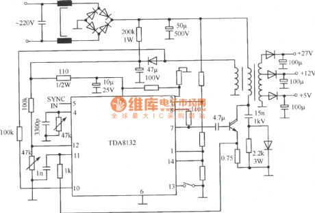
View full Circuit Diagram | Comments | Reading(813)
TDA8130 typical application circuit (switching regualted power supply)
Published:2011/4/20 6:25:00 Author:May | Keyword: typical application, switching regualted power supply
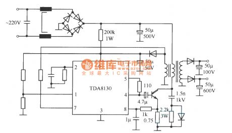
View full Circuit Diagram | Comments | Reading(1246)
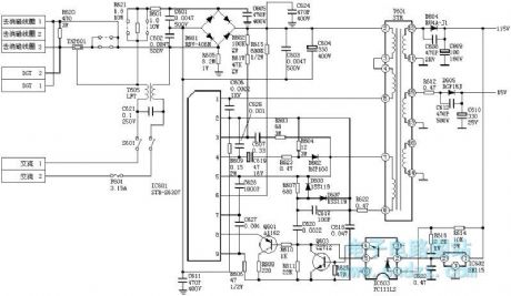
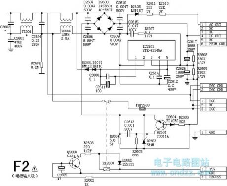
STR6309 power supply
Published:2011/4/20 6:23:00 Author:May | Keyword: power supply
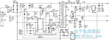
View full Circuit Diagram | Comments | Reading(1351)
SONY KV2185 power supply
Published:2011/4/20 6:22:00 Author:May | Keyword: power supply
View full Circuit Diagram | Comments | Reading(2156)
SONY KV2184 power supply
Published:2011/4/20 6:22:00 Author:May | Keyword: power supply

View full Circuit Diagram | Comments | Reading(805)
SONY G3F-K power supply 2
Published:2011/4/20 6:21:00 Author:May | Keyword: power supply
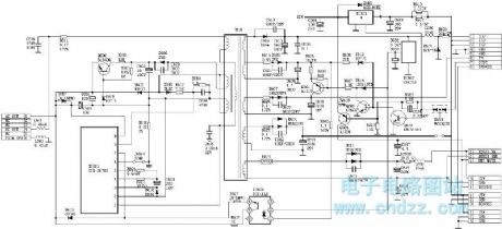
View full Circuit Diagram | Comments | Reading(740)
SONY G3F-K power supply 1
Published:2011/4/20 6:20:00 Author:May | Keyword: power supply
View full Circuit Diagram | Comments | Reading(597)
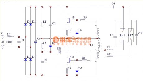
Shengguang 15W electron ballast circuit
Published:2011/4/20 6:28:00 Author:May | Keyword: Shengguang, 15W, electron ballast
View full Circuit Diagram | Comments | Reading(621)
Duplex tube electron ballast circuit
Published:2011/4/20 6:29:00 Author:May | Keyword: Duplex tube, electron ballast
View full Circuit Diagram | Comments | Reading(620)
One kind of electron ballast circuit principle diagram
Published:2011/4/20 6:30:00 Author:May | Keyword: electron ballast
View full Circuit Diagram | Comments | Reading(672)
20W fluorescent light electron ballast using MJE13005×2
Published:2011/4/20 6:32:00 Author:May | Keyword: 20W, fluorescent light, electron ballast
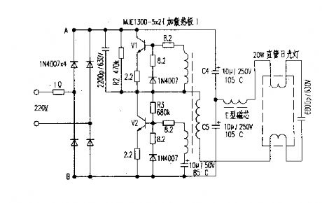
View full Circuit Diagram | Comments | Reading(8423)
Automatic opening/closing circuit (Rph is photoresistance)
Published:2011/4/20 6:34:00 Author:May | Keyword: Automatic opening/closing, Rph, photoresistance
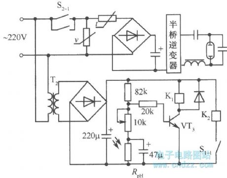
View full Circuit Diagram | Comments | Reading(673)
Simpleset standard Li-ion battery charger
Published:2011/4/20 6:34:00 Author:May | Keyword: Li-ion battery charger
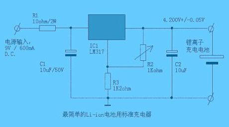
View full Circuit Diagram | Comments | Reading(1296)
Automatic plumbic acid charging circuit diagram
Published:2011/4/20 6:36:00 Author:May | Keyword: Automatic, plumbic acid, charging
View full Circuit Diagram | Comments | Reading(843)
Two-way output normal shock type 150W precision switch stabilized voltage supply
Published:2011/4/20 5:07:00 Author:May | Keyword: Two-way output, normal shock type, 150W, precision switch, stabilized voltage supply
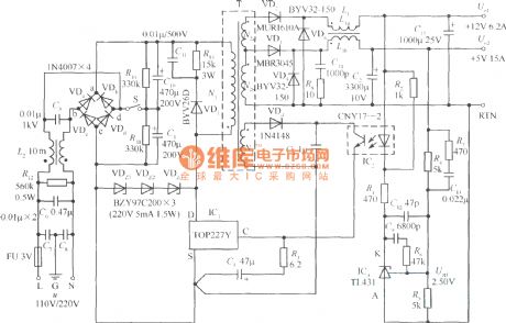
+5V, +12V two-way output normal shock type 150W precision switch stabilized voltage supply is shown in the diagram. This power supply uses one pieces of TOP227Y(IC1), linearity optical couple CNY17-2 (IC2, the production of Germany Telefunken company) , adjustable precision parallel regulator TL431 (IC3). AC input voltage is 110V/220V. When it is low voltage input, power supply's efficiency can reach 77% (typical value).
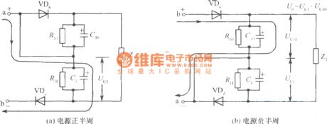
S is power supply choosing switch. When S is closed, it is choosing AC voltage IIOV voltage doubling rectifying circuit. Its working principle is shown in the following diagram. Supposing the positive half period a point of AC is positive potential, b point is negative potential, at this time, the diode VDb and VDd on rectifier bridges is breaking over, VDa an VDd is cutting off, shown in diagram (a). 110V AC can charge to C1 according to the following ways: u→a→C1→VDc→b, it can charge Uc1 to about ×llOV=155V, its polarity is that up end is positive and down end is negative. When in negative half period, b point is positive potential, a point is changing to negative potential, the equivalent circuit is shown in diagram (b). At this time, VDa, VDd is breaking over, VDb, VDc is cutting off, the current can charge to C10 according to following ways: u→b→VDa→C10→a, it can make Uc10≈115V, and the polarity is also that up end is positive and down end is negative.
(View)
View full Circuit Diagram | Comments | Reading(3303)
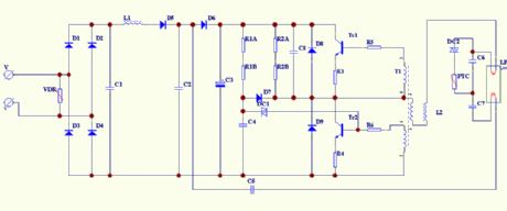
Small size middle power switching powr supply (10W-60W circuit diagram)
Published:2011/4/20 3:43:00 Author:May | Keyword: Small size, middle power, switching powr supply, 10W-60W
Small size middle power switching powr supply (10W-60W circuit diagram)---amplifying circuit diagram
(View)
View full Circuit Diagram | Comments | Reading(1284)
Push pull circuit using complementary transistor and CMOS driving stage
Published:2011/4/19 22:38:00 Author:May | Keyword: Push pull, complementary transistor, CMOS driving stage
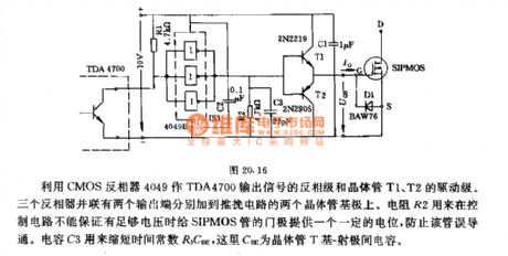
It is using CMOS inverter 4049 as driving stage of inverter stage of TDA4700 's output signal and transistor T1, T2. Three inverters are parallel. Two output ends among them are separately adding to the base of two transistors in push pull circuit. Resistor R2 is used for controlling the circuit. When it can not guarantee enough voltage for SIPMOS tube's gate pole to offer a fixed potential, it can prevent the error breaking over of this tube. Capacitor C3 is used for shorting time constant R2CBE. Here, CBE is capacitor between base-emitter of transistor T. (View)
View full Circuit Diagram | Comments | Reading(1130)
| Pages:2050/2234 At 2020412042204320442045204620472048204920502051205220532054205520562057205820592060Under 20 |
Circuit Categories
power supply circuit
Amplifier Circuit
Basic Circuit
LED and Light Circuit
Sensor Circuit
Signal Processing
Electrical Equipment Circuit
Control Circuit
Remote Control Circuit
A/D-D/A Converter Circuit
Audio Circuit
Measuring and Test Circuit
Communication Circuit
Computer-Related Circuit
555 Circuit
Automotive Circuit
Repairing Circuit