
Index 108
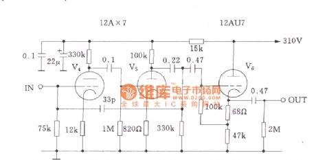
McIntosh-C22 tube amplification and output stage circuit diagram
Published:2011/9/25 21:41:00 Author:Ecco | Keyword: tube amplification , output stage
View full Circuit Diagram | Comments | Reading(1572)
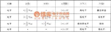
5G7556 CMOS time-base internal equivalent circuit diagram
Published:2011/9/25 22:06:00 Author:Ecco | Keyword: CMOS time-base , internal equivalent
View full Circuit Diagram | Comments | Reading(745)
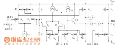
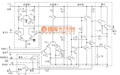
5G1555 equivalent circuit diagram produced by Shanghai components 5th factory
Published:2011/9/25 22:03:00 Author:Ecco | Keyword: equivalent circuit
View full Circuit Diagram | Comments | Reading(703)
Double-tube single-resistance independent circuit diagram
Published:2011/9/25 21:06:00 Author:Ecco | Keyword: Double-tube, single-resistance , independent
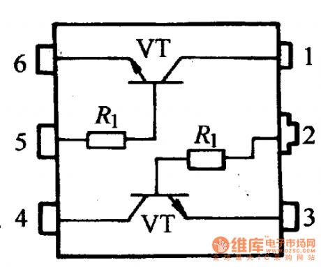
The main varieties of resistance transistor is a small power tube, which is widely used in household appliances and other electronic devices for electronic switch or inverter. Some band-stop tube containing two transistors, leads 5-6 feet.
(View)
View full Circuit Diagram | Comments | Reading(1038)
Using real USB chip and the ISP2 of M8
Published:2011/9/18 21:23:00 Author:Ecco | Keyword: Real, USB chip, ISP2
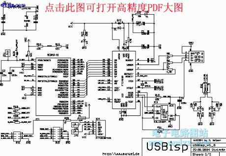
View full Circuit Diagram | Comments | Reading(738)
The circuit and sound code of AT89C2051 driving stepping motor
Published:2011/8/2 1:19:00 Author:Ecco | Keyword: sound code, driving stepping motor
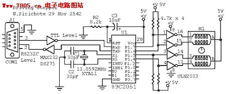
View full Circuit Diagram | Comments | Reading(1723)
TMS320LF2407DSP Typical customers board principle diagram(PROTEL99 principle diagram)
Published:2011/8/2 1:18:00 Author:Ecco | Keyword: Typical, customers board
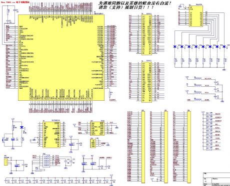
View full Circuit Diagram | Comments | Reading(735)
A watchdog circuit
Published:2011/9/19 1:14:00 Author:Ecco | Keyword: watchdog , circuit
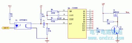
The circuit is shown as above: when the circuit works, it needs to add the reset pulse to the CD4060 regularly, we can guarantee Q1 being in cutting off state, so that the tube controlled by the NMOS will be in conduction state to provide power to the processor circuitry.
The circuit has the advantages of long timing time with over a few minutes; you can take a long time to initialize the system. The power passing R2, C1, R3 automatically provides a reset pulse to the counter to ensure that there is output of Vout. The circuit costs low.
The biggest drawback of the circuit is feeding dog pulse requires wide band.
(View)
View full Circuit Diagram | Comments | Reading(1412)
The boost converter circuit diagram composed of LTC3401
Published:2011/8/31 2:20:00 Author:Rebekka | Keyword: boost converter
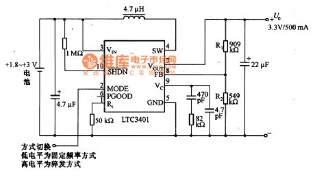
Boost converter circuit is composed of LTC3401. LTC3401 is a circuit which has all the functions needed by boost power supply. it can start to work with 1V input voltage. It costs a low current with38μA. Input voltage range is 1 ~ 5V, output voltage is set in 2.6 ~ 5Vby R1 and R2. LTC3401 uses 2-pin mode switching terminal. The control signal can be applied. When the control signal is low, LTC3401 works for the fixed frequency. Ituses burst working mode when the level is high. (View)
View full Circuit Diagram | Comments | Reading(1048)
The buck converter circuit diagram composed of LM305
Published:2011/8/31 2:15:00 Author:Rebekka | Keyword: buck converter
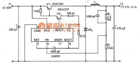
The buck converter circuit is composed of LM305. It uses self-excited buck DC / DC converter. Input voltage is +12 ~ +30 V, output voltage is +5 V, maximum output current is 2A. The internal LM3O5 is a robot control integrated circuit composed of a reference voltage, operational amplifiers, driver circuit. Output voltage is set to 3V or less. It can not be switching. The loss of VT increases. Output voltage U. = [(R1 + R2/R2] UREF, UREF = 1.8V. (View)
View full Circuit Diagram | Comments | Reading(3579)
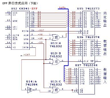
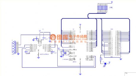
USB to parallel, serial circuit diagram(ch341)
Published:2011/9/18 21:34:00 Author:Ecco | Keyword: USB , parallel, serial
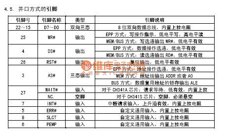
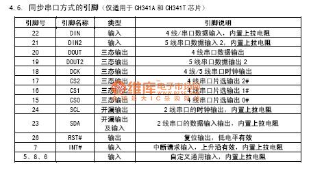
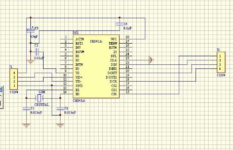
View full Circuit Diagram | Comments | Reading(7018)
Hard disk control circuit and the original program
Published:2011/9/18 23:03:00 Author:Ecco | Keyword: Hard disk, control circuit , original program
In the program, all hardware-related parameters is defined at the beginning of the program, when it is transplanted to other types of microcontrollers, the pins defination needs to be simplily changed. When it is used, the corresponding parameters need to be modified according to your hard (there are comments in the program). Firstly, you should connect the circuit (very simple), then the chip is burned into the process. Firstly ,the hard is connected to power, and then you can open any serial debugger to set the baud rate in 57600bps, and then you can run the microcontroller.
(View)
View full Circuit Diagram | Comments | Reading(1704)
The current loop interface circuit diagram of AD694 being used as D / A converter
Published:2011/9/18 22:35:00 Author:Ecco | Keyword: current loop , interface circuit, D / A converter
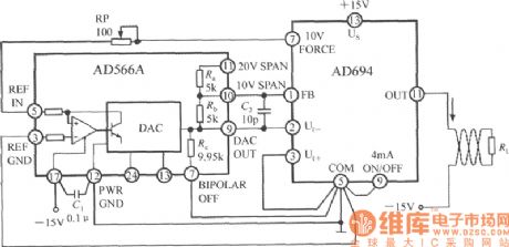
The current loop interface circuit diagram of AD694 multi-functional sensor signal conditioner being used as D / A converter.
The current loop interface of AD694 being used as D / A converter (DAC) can achieve the conversion of digitalvalue →voltage signal →current signal . DAC's current loop interface circuit is shown as the chart. AD566A is high-speed 12-bit DAC, its output (DAC OUT) is connected to AD694's UI-end, UI + is grounded. AD694 uses ± 15V dual supplies, and provides reference voltage to the AD566A. Internal resistor network of AD566A will set AD694 with 10V full scale input. C2 is the frequency compensation capacitor. RP is the full scale adjusting potentiometer, it has no need to use a fixed adjustment 50Ω resistor to replace the potentiometer.
(View)
View full Circuit Diagram | Comments | Reading(2855)
The LA4505 IC typical application circuit
Published:2011/9/19 1:32:00 Author:Ecco | Keyword: typical application , IC
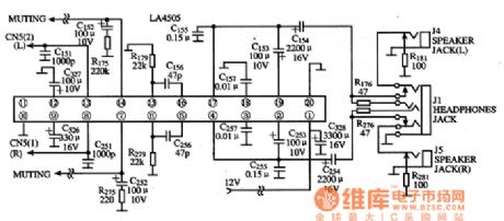
The typical application circuit
The typical application circuit of LA4505 IC is shown as the chart, the left and right audio signalsare input from the foot and pin ⑧ of LA4505 and it is amplified and output from ④ feet to drive the speaker power, and the power can reach ten 8W +8W (RL30).
(View)
View full Circuit Diagram | Comments | Reading(4545)
Integrated circuit diagram of TDA9112-I2C bus control row / field scanning
Published:2011/9/19 1:18:00 Author:Ecco | Keyword: bus control, row , field , scanning , integrated circuit
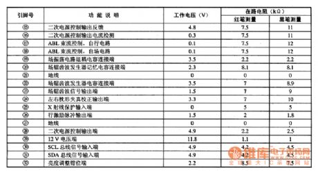
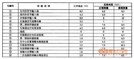
TDA9112 is the bus control row / field scanning integrated circuit produced by Philips, it is widely used in color displays, such as color display of Tsinghua Tongfang. 1. Featuresand functionTDA9112 IC includes I2C bus interface circuit, the line oscillator circuit, field oscillation and the sawtooth wave generating circuit, left and right pincushion correction circuit, the line excitation circuit, PLL circuit, the same frequency signal processing circuit, ABL beam current system circuit, X-ray protection circuit, and other auxiliary functions circuit. 2. Pin functions and dataTDA9112 IC uses 32-pin dual in-line package, the pin functions and the number are shown in Table 1. Table 1 shows TDA9112 integrated circuit pin functions and data.
(View)
View full Circuit Diagram | Comments | Reading(995)
The driver circuit diagram of glow numerating tube
Published:2011/9/19 1:17:00 Author:Ecco | Keyword: glow numerating tube , driver circuit
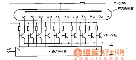
The glow numerating tube can be driven by a strong electric field, so it needs to be equipped with an electronic switch between decoder and the glow digital tube. The VT1-VT10 shown in the circuit is the switch circuit that composed of transistors. (View)
View full Circuit Diagram | Comments | Reading(1354)
Power factor compensation schematic circuit diagram
Published:2011/9/14 21:11:00 Author:Rebekka | Keyword: Power factor compensation
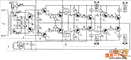
The controller is divided into measurement part, Enlarged part of the DC, executing part and power supply part by dotted line. The operation is as follows: Converting the phase displacement between AC voltage and current into DC voltage signal. Then making DC driver signal amplification work in sections, theninput or remove to compensation capacitor.
(View)
View full Circuit Diagram | Comments | Reading(1239)
Dual op amp basic subtraction circuit composed of ICL7622
Published:2011/8/22 22:32:00 Author:Rebekka | Keyword: Dual op amp, basic subtraction
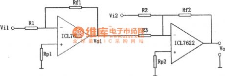
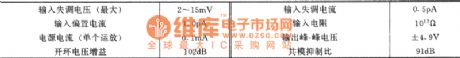
Dual op amp basic subtraction circuit composed of ICL7622 is shown as above.
The device used in the circuit is ICL7622 (or CF7622) which is a monolithic CMOS dual op amp dual low-power, and its working power voltage is ± 0.5 ~ ± 8V. The input current is very small. The device also has the features of internal compensation for zero offset, offset fixed and so on. The main typical parameters of ICL7622are shown as above. (View)
View full Circuit Diagram | Comments | Reading(673)
Wiring diagram of DC meter
Published:2011/9/18 20:47:00 Author:Ecco | Keyword: wiring diagram , DC meter
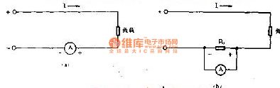
Ammeter is used to measure the current in the circuit for the electricians, and meter is connected to tested circuit in series. The positive pole of DC ammeter should be connected to the positive terminal of DC power supply. The limiting amount of the instrument shoulf be 1.5 to 2 times of measuring current. Figure A shows the direct access method of DC ammeter, and b is the access method of the DC ammeter with external shunt.
(View)
View full Circuit Diagram | Comments | Reading(727)
The converter circuit diagram with MAX668
Published:2011/8/2 1:12:00 Author:Ecco | Keyword: converter, MOSFET
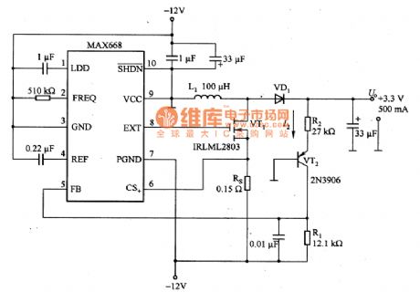
Figure shows the converter circuitwith MAX668, and MAX668 is a core component of the circuit, and it is a switching power supply integrated controller with PWM operation. The circuit shown in Figure 5 is a boost circuit which can switch -12V voltage into +3.3 V or +5 V. The RS in the circuit is sensitive resistor, which can limit the peak current to 12OmA, and N-channel switch MOSFET VT1 uses the low-cost devices with logic level.
(View)
View full Circuit Diagram | Comments | Reading(1298)
| Pages:108/471 At 20101102103104105106107108109110111112113114115116117118119120Under 20 |
Circuit Categories
power supply circuit
Amplifier Circuit
Basic Circuit
LED and Light Circuit
Sensor Circuit
Signal Processing
Electrical Equipment Circuit
Control Circuit
Remote Control Circuit
A/D-D/A Converter Circuit
Audio Circuit
Measuring and Test Circuit
Communication Circuit
Computer-Related Circuit
555 Circuit
Automotive Circuit
Repairing Circuit