
Index 103
The circuit diagram of DKIOOOT OOK315 MHz transmitter
Published:2011/10/18 3:48:00 Author:Ecco | Keyword: MHz transmitter
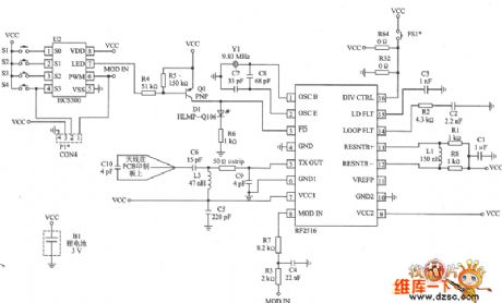
View full Circuit Diagram | Comments | Reading(744)
RS232C Pin and diagonal connection
Published:2011/10/18 3:44:00 Author:Ecco | Keyword: Pin , diagonal connections
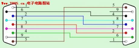
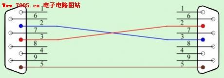

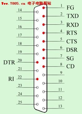
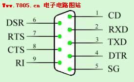
FG, SG-Frame Ground- the ground wire connected to the machineTXD, SD-Transmitted Data- data output line RXD, RD-Received Data-data input line RTS, RS-Request to Send- Request to Send dataCTS, CS-Clear to Send data- it responds to other permission and tells the other party that it can send. DSR, DR-Data Set Ready- it can inform the machine is in standby state.DTR, ER-Data Terminal Ready- Data Terminal is informed on standby state.CD, CD-Carrier Detect-carrier detection, which is used to confirm receipt of the Modem carrierSG, SG-Signal Ground-Signal ground line (The signal line is the zero standard line) (View)
View full Circuit Diagram | Comments | Reading(1155)
Self-made AVRISP download rom recorder
Published:2011/10/18 3:39:00 Author:Ecco | Keyword: Self-made , AVRISP, download , rom recorder
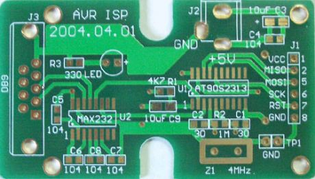
Comparing with an ISP download cable with 74LS244 parallel port, the line and principles of this AVRISP is slightly more complicated. But it has advantages:the serial port's download performanceis more stable than a parallel port, it needs 8 seconds to complete by testing 16k program, and its speed is also fast when it is improved 3.6-firmware. In addition, to the users who are short for parallel port, it is a good choice.
(View)
View full Circuit Diagram | Comments | Reading(726)
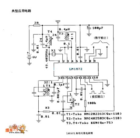
Logic box circuit diagram of LMl872
Published:2011/10/18 3:42:00 Author:Ecco | Keyword: logic box
View full Circuit Diagram | Comments | Reading(659)
Digital displaying photoelectric counter circuit diagram
Published:2011/9/26 21:50:00 Author:Rebekka | Keyword: Digital displaying , photoelectric counter
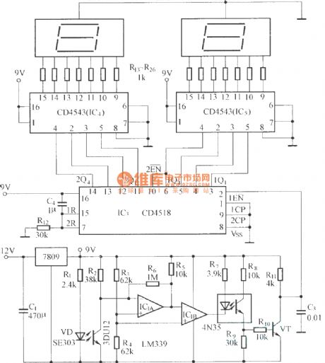
The circuit has optical input circuit (VD, 3DU12), pulse forming circuit (IC1A, IC1B form the voltage comparator; optical coupler; transistor switching circuit) and counting and display circuit. (View)
View full Circuit Diagram | Comments | Reading(2657)
Digital Potentiometers X9511 circuit diagram
Published:2011/9/16 0:50:00 Author:Rebekka | Keyword: Digital Potentiometers
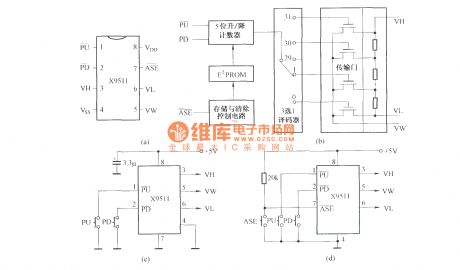
X9511 is a of non-volatile Digital Potentiometer with digital integrated circuit manufacturing process. Its internal binary counter is composed of five binary counter, five-bit rewritten read-only memory (that E2PROM), storage and clear control circuit, thirty-two selected one decoder circuit, transmission gate and resistor arrays and other components. Pin and functionare shown as above. (View)
View full Circuit Diagram | Comments | Reading(1451)
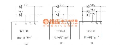
The attachment method of TC9148 user code
Published:2011/9/27 21:13:00 Author:Rebekka | Keyword: attachment method , user code
View full Circuit Diagram | Comments | Reading(733)
BA1404 Internal schematic diagram
Published:2011/9/27 1:56:00 Author:Rebekka | Keyword: Internal schematic diagram
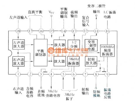
BA1404 IC is a dedicated FM transmitter circuit.
(View)
View full Circuit Diagram | Comments | Reading(1344)
VD5026/27 pinout function circuit diagram
Published:2011/9/27 21:39:00 Author:Rebekka | Keyword: pinout function
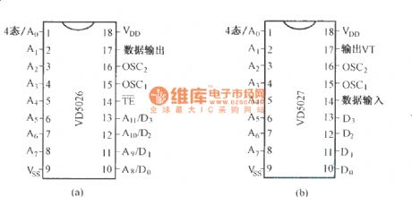
Integrated digital coding circuit VD5026 and its supporting decoding circuit VD5027 are a pair of commonly used digital code, decoding circuit. The pinout function circuit diagram is shown as the chart. (View)
View full Circuit Diagram | Comments | Reading(1072)
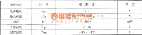
YN5101/5201 Multi-channel infrared remote control encoder and decoder typical application circuit diagram
Published:2011/9/27 21:36:00 Author:Rebekka | Keyword: infrared remote control , encoder and decoder, typical application
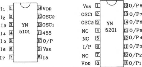
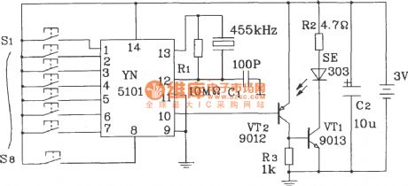
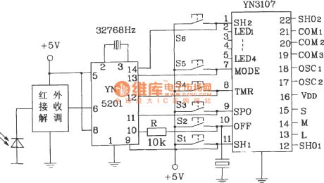
YN5101/5201 encoder / decoder extreme working parameters: Supply voltage is0 ~ 6v; input / output voltage: (Vss-0.2V) / (VDD +0.3 v); maximum power consumptionis 500mW; Operating Temperature is -20 ~ +70 ℃; Storage temperature is-55 ~ +125 ℃.
Typical application circuit YN5101 encoding device.
Typical application circuit decoding device YN5201.
Infrared receiver demodulation circuit can use a dedicated infrared modules or infrared preamplifier IC dedicated to form infrared demodulation circuit. The general infrared preamplifier IC models are: CX2106A, μPCI373HA, μPCI490 and KA2184, etc.
(View)
View full Circuit Diagram | Comments | Reading(5237)
YN5048 Infrared transmitter IC typical application circuit diagram
Published:2011/9/27 21:27:00 Author:Rebekka | Keyword: Infrared transmitter IC , typical application
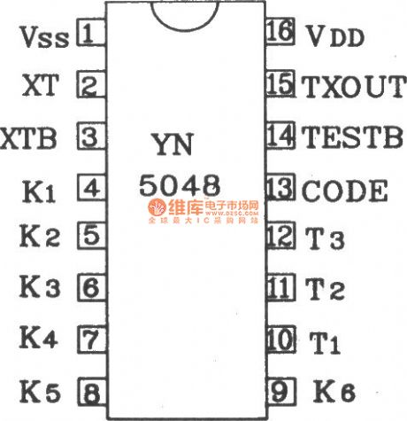
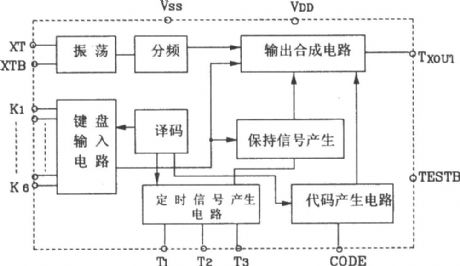
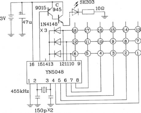
The internal YN5048 infrared remote control transmitter uses COMS structure, operating voltage range iswide (1.5 ~ 5.0V), and it is mainly used in televisions, stereos, video recorders and a variety of remote control circuits. The similar models areBL9148, TC9148.
YN5048 shape pin map.
YN5048 internal block diagram.
YN5048 infrared remote control transmitter limit operating parameters.
Typical application circuit of YN5048 infrared emission IC.
(View)
View full Circuit Diagram | Comments | Reading(1140)
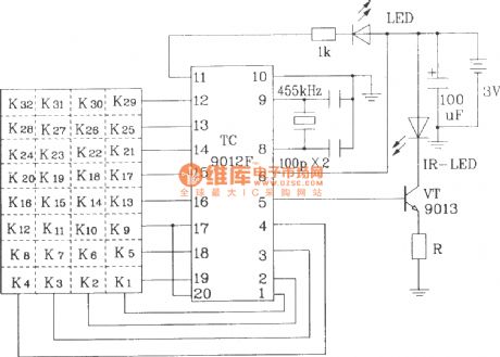
Typical infrared emission application circuit diagram composed of TC9012F
Published:2011/9/27 21:16:00 Author:Rebekka | Keyword: typical infrared emission , application circuit
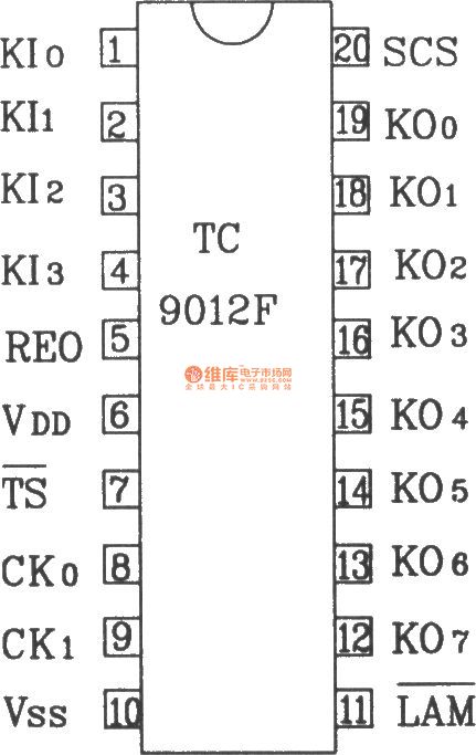
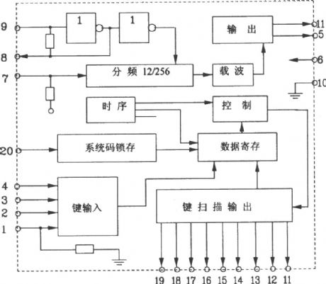
TC9012 is a special off screen remote control code transmitter. It includes oscillator, divider timing generator, system code latch, data storage, key scan input, key scan output, the carrier control and output units. Its internal 8-bit system code setting can be achieved with 256 points while operating the transmitter and the interfering transmitter.
TC9012F shape pin map.
TC9012F infrared emission constitutes a typical application circuit is shown as below.
(View)
View full Circuit Diagram | Comments | Reading(1749)
TWH9238 Self-locking and interlocked hybrid application circuit diagram
Published:2011/10/18 1:54:00 Author:Rebekka | Keyword: Self-locking and interlocked hybrid application
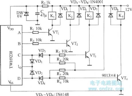
In this circuit, A, B channels are interlocking type output. At the same time, one way plays the controlling role. C, D channels are non-locking output connection, relays K3, K4 use self-locking relays. If it uses a common relay, it should plus a set of connected bistable circuit behind VT3, VT4(or at the output C, D). (View)
View full Circuit Diagram | Comments | Reading(1170)
TWH9238 interlock application circuit diagram
Published:2011/10/18 1:53:00 Author:Rebekka | Keyword: interlock application circuit
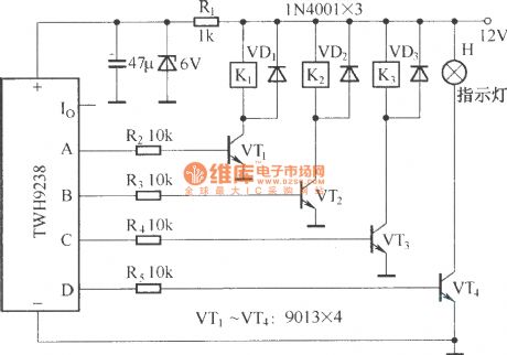
The output terminals A, B, C, D of TWH9238 transmitter pass the transistor drive and drive a DC relay. One output of the circuit plays the role of control at one time. D output connects toan indicator to show shutdown mode. (View)
View full Circuit Diagram | Comments | Reading(1078)
The circuit composed of CSJ-T300A/CSJ-R02A and SCM
Published:2011/9/16 1:15:00 Author:Rebekka | Keyword: SCM
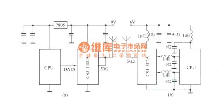
CSJ-T300A and CSJ-R02Aare miniature ultra-long range wireless remote control / data transfer components. CSJ-T300A is transmitter module without the launch code components. The internal circuit is composed of table resonator oscillator, buffer promoting stage, high-frequency power amplifier and amplitude shift keying (ASK) modulator. CSJ-R02A is the SAW frequency stabilized superheterodyne receiver module. The core component of the internal circuit is RX3310A monolithic superheterodyne receiver circuit. If it is matching with the SAW resonator with the frequency stabilized bylocal oscillator. Work is very stable and reliable. The inductor connection is set for SCM system to suppress the received interference. (View)
View full Circuit Diagram | Comments | Reading(699)
Frequency meter with 10Hz to 2MHz
Published:2011/8/22 20:31:00 Author:muriel | Keyword: Frequency meter , 10Hz to 2MHz
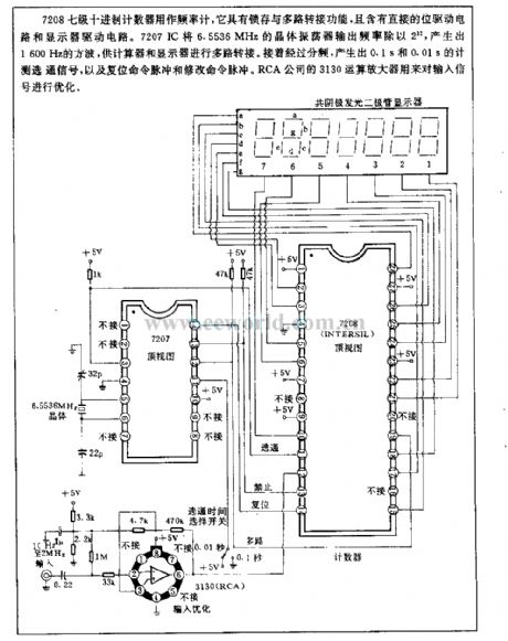
7208 seven metric system counter is used for frequency meter, it has latch and multiplexing function, and contains direct drive circuit and display driver circuit. 7207IC is divided the output frequencyof6.5536 MHz crystal oscillator by2 12which produces the 1600Hz square wave for calculator and display connection multiplexing. After fractional frequency, it produces 0.1 s and 0.01 s measurement gating signal and thenchooses communication and reset command pulse, modify ordered pulse. RCA company's 3130 operational amplifier is used for optimize the input signal. (View)
View full Circuit Diagram | Comments | Reading(3028)
Application Circuit Design of Fuji IGBT Intelligence Module
Published:2011/8/22 21:15:00 Author:muriel | Keyword: Fuji IGBT, Intelligence module , application circuit design
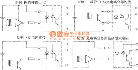
1.Photoelectric coupler drive circuit
Peripheral control circuit mainly aims at the single-chip control system of weak current control part, because the IPM module directly connects the distribution system, therefore, it must use segregation device to isolate the IPM module and the weak current circuit of control part, to protect the single-chip microcomputer control system. Meanwhile, the working conditions of IPM module depend largely on the right, effective and timely control signals. So,itdesigns a fine photoelectric coupler control circuit, whichis also the key to work normally IPM module, and it isshown as the chart.
2.Buffer circuit
(View)
View full Circuit Diagram | Comments | Reading(902)
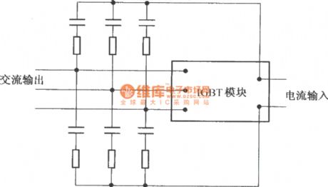
Grid overvoltage protection circuit
Published:2011/8/22 21:14:00 Author:muriel | Keyword: Grid , overvoltage protection circuit
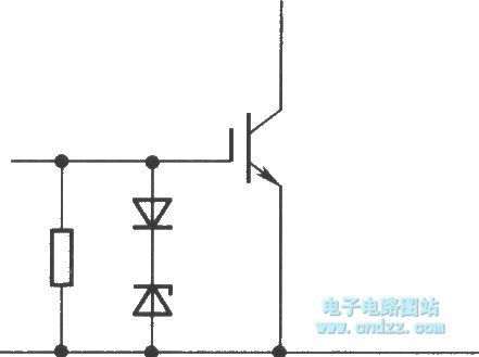
Reasons for grid's overvoltage:
1. Static electricity on the grid capacitance cancause overvoltage.2. Capacitance mueller effect causes grid overvoltage.To prevent the IGBT grid-emitter from overvoltge, a resistance with dozen kilohm should be connected between the grid and emitter of IGBT in parallel. As the figure is shown, the resistance should beclosed to the grid and emitter. (View)
View full Circuit Diagram | Comments | Reading(1631)
KL3 microwave electronic switching circuit diagram
Published:2011/10/17 21:57:00 Author:Rebekka | Keyword: microwave electronic switching circuit
KL3 microwave electronic switch is made by using doppler effect of electromagnetic wave theory. The entire circuit is encapsulated in a plastic case. The outside has four lead lines. 2 of red lead lines areconnected to AC 220V power supply. 2 green lead lines are connected to controlled load. It is suitable for automatic control of lighting or anti-theft alarm device. (View)
View full Circuit Diagram | Comments | Reading(1283)
TDA8145 pincushion correction circuit diagram
Published:2011/10/17 21:24:00 Author:Rebekka | Keyword: pincushion correction
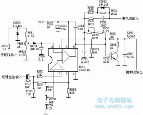
TDA8145 is a widely used pincushion correction special IC. Its basic working principle is as follow: Field sawtooth voltageis sentto the N551's (2) feet by passing C592, R550. VR552 is the pillow distortion correction adjustment potentiometer. Adjusting it essentially can change the the amount of negative feedback from N551's 5 feet to 7, and it changes the pin 5 sparabolic wave output voltage rangeto make themoderate correction. There is not distortion of grating to keep rectangular state. VR553 is theline adjusting potentiometer.
(View)
View full Circuit Diagram | Comments | Reading(10287)
| Pages:103/471 At 20101102103104105106107108109110111112113114115116117118119120Under 20 |
Circuit Categories
power supply circuit
Amplifier Circuit
Basic Circuit
LED and Light Circuit
Sensor Circuit
Signal Processing
Electrical Equipment Circuit
Control Circuit
Remote Control Circuit
A/D-D/A Converter Circuit
Audio Circuit
Measuring and Test Circuit
Communication Circuit
Computer-Related Circuit
555 Circuit
Automotive Circuit
Repairing Circuit