
Communication Circuit
Index 5
20 kbit optical cable receiving circuit
Published:2011/12/1 20:30:00 Author:May | Keyword: 20 kbit optical cable, receiving
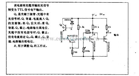
This circuit turns theoptical signal transmitted by optical cable to TTL signal level output.
Q1 is photistor. When the optical cable receives signal, Q1 is breakover, the current flows into emitter of Q2. After being enlarged by Q2, the current makes Q3 breakove and Q4 close, the circuit outputs high level. When the optical cable can not receive signal, Q1 is closed. There is no current flowing into Q2, and Q3 is closed, Q4 is breakover, and the circuit output is in low level.
R1 is used for adjusting the operation point of Q3. (View)
View full Circuit Diagram | Comments | Reading(1308)
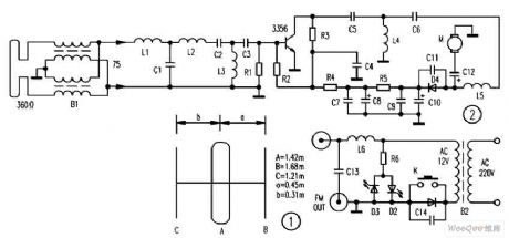
FM broadcast special-purpose electric wire circuit diagram
Published:2011/10/20 21:09:00 Author:Rebekka | Keyword: FM broadcast , special-purpose electric wire
View full Circuit Diagram | Comments | Reading(1664)
Transmitting and receiving wireless calls ward display circuit (M303S/M303R)
Published:2011/10/18 1:50:00 Author:Rebekka | Keyword: Transmitting and receiving, wireless calls , ward display
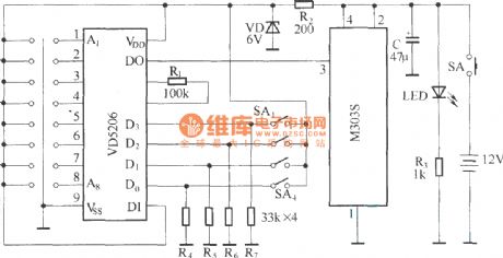
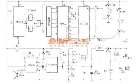
This circuit uses the wireless transmission and digital radio transceiver module M303S/M303R with stable performance, digital decoders VD5026/VD5027. It is stable and reliable to display the call number or room number of beds. It is easy to install. RF transmission power of the circuit is very small. It does not affect the normal operation of medical equipment. Ward Wireless call system is composed of wireless calling transmitter set in ward and radio receiver display set in care duty room. The circuit is shown as below.
Monitors radio receiver circuit is shown as below.
(View)
View full Circuit Diagram | Comments | Reading(2490)
DTMF wireless paging system circuit diagram
Published:2011/10/18 1:36:00 Author:Rebekka | Keyword: wireless paging system , DTMF
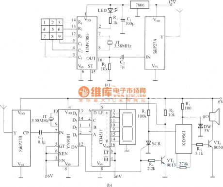
IT usesDTMF encoder output dual tone multi-frequency coded signal to modulate the transmitted carrier frequency. It can form a DTMF encoded radio paging system. The circuit uses DTMF encoding UM97085 and decoding circuit YN9101 circuit to form a small wireless paging system for small internal paging. It is convenient and economical. It is shown in the figure, in which (a) shows the radio transmitting DTMF encoding circuit. Figure (b) shows the radio receiver demodulation, DTMF decoding and reproducing sound signal circuits. (View)
View full Circuit Diagram | Comments | Reading(5295)
The basic radio SR circuit diagram composed of F36-F/J
Published:2011/10/18 1:31:00 Author:Rebekka | Keyword: basic radio SR
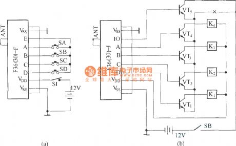
F36-F / J is a pair of digitally encoded radio frequency transceiver components, and the named carrier frequency is 36MHz. F36-F / J components are used in encoding / decoding circuit PT2262/PT2272.
F36-F / J constitutes the basic radio transceiver circuit, whichis shown as above. (View)
View full Circuit Diagram | Comments | Reading(3620)
The communication circuit of monitoring module and rectification module
Published:2011/8/22 21:16:00 Author:muriel | Keyword: monitoring module, rectification module
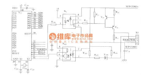
As shown is the monitoring module and rectification module of communication circuit. Optocoupler N9and N452 provide isolation between microprocessor D211 and rectification module, the N9 isisolated the send buffer V15 and V10, the send buffer V15 and V10 are designed for communcationdrive capability of 100 rectification module, N451 is a HG optocoupler buffer, it is receiving the rectification module's signals. (View)
View full Circuit Diagram | Comments | Reading(1305)
810E computer motherboard circuit diagram 22
Published:2011/10/26 1:56:00 Author:Ecco | Keyword: computer motherboard
View full Circuit Diagram | Comments | Reading(1391)
USA CDMA application circuit composed of RF2162
Published:2011/10/23 21:51:00 Author:May | Keyword: USA CDMA
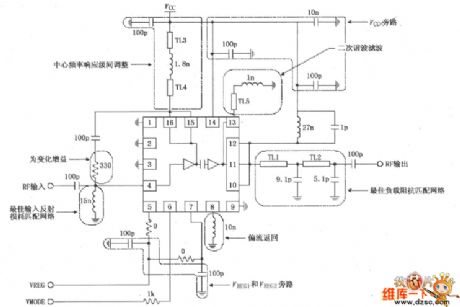
The diagram is USA CDMA application circuit composed of RF2162. Radio-frequency signal (RF) isinput by pin 4, enlarged by preamplifier, final power amplifier, then output by pin 10, 11, 12. Pin 4 is directly coupling with inside amplifier, so itsuggests to add an UHF blocking coupling capacitor.Pin 13 is used as thesecond harmonics filter circuit, and it uses transmission line or inductanceandchip capacitor to make up filter with resonance at 2f0, it can offer low impedance path to second harmonics and short-circuit second harmonics effectively. Pin 14 is used as the final power amplifier power supply end, which offers bias current. Pin 5 connects to thefirst step enable voltage VREG1, when this pin is low level, the circuit shuts off; when it is inhigh level ( 2.8V),all circuit worksin thestandard state, and pin 5is connectedto 100pF high frequency filter capacitor. Pin 6 connects toanalog bias control pin VMODE, when pin 6 is 0V, itoffers theminimum bias.
(View)
View full Circuit Diagram | Comments | Reading(1714)
Anti-lost children warning circuit diagram(transceiver module composed of RCMlA / RCMlB)
Published:2011/10/20 2:30:00 Author:Rebekka | Keyword: Anti-lost children
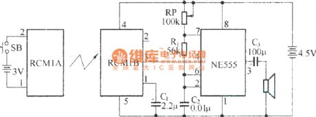
The circuit is composed of the transmitter and receiver, and the core componentsare RCM1A and RCM1B. (View)
View full Circuit Diagram | Comments | Reading(1696)
820e computer motherboard circuit diagram 32
Published:2011/10/24 20:25:00 Author:Ecco | Keyword: computer motherboard
View full Circuit Diagram | Comments | Reading(972)
Typical remote control transmitter and receiver application circuit composed of LC219/LC220A
Published:2011/10/17 22:01:00 Author:Rebekka | Keyword: remote control , transmitter, receiver
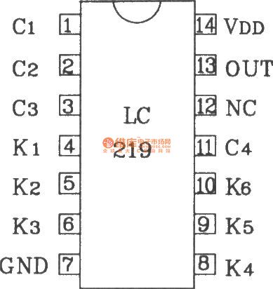
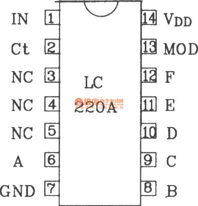
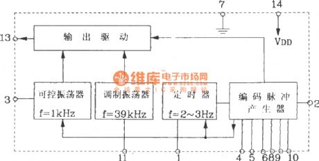
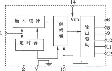
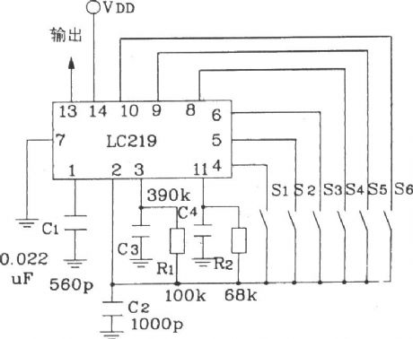
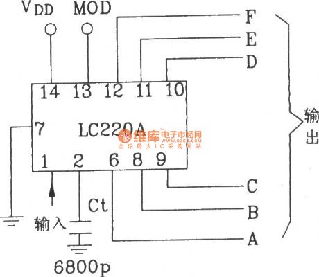
LC219/LC220A is a multi-function remote control transmitter / receiver integrated circuit. It is generally used in electric fans shift, wave side of the conversion, home appliances and toys, remote control rolling circuit.
LC219 transmitter chip block diagram
LC219 transmitter chip supply voltage range is 2.5 ~ 6V; Quiescent operating current is less than 5μA; Output drive current IoH ≥ 2mA, IoL ≥ 300μA. It is applicable to high-driven work NPN transistor; Repetition rate of the internal timer is 2 ~ 3Hz, controllable oscillation frequency is lkHz, duty cycle is 50%, pulse width is 0.5ms: modulation oscillation frequency range is 32 ~ 48kHz, Generally it uses 39kHz appropriate election. LC220A receiver chip supply voltage is 4.5 ~ 9V; Quiescent operating current is less than 5μA; Each output drive current is IoH ≥ 2mA, Ioc ≥ lmA; Output short-circuit current is IOH (S) ≥ 8mA, IOL (S) 5mA. It can be connected with LED drive directly or transistors.
(View)
View full Circuit Diagram | Comments | Reading(2234)
Four-action RF remote transmitter and receiver circuit composed of KIA6933S/6957P
Published:2011/10/17 21:55:00 Author:Rebekka | Keyword: four-actions RF remote, transmitter , receiver
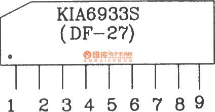
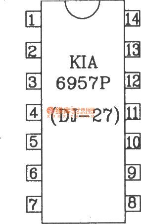
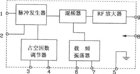
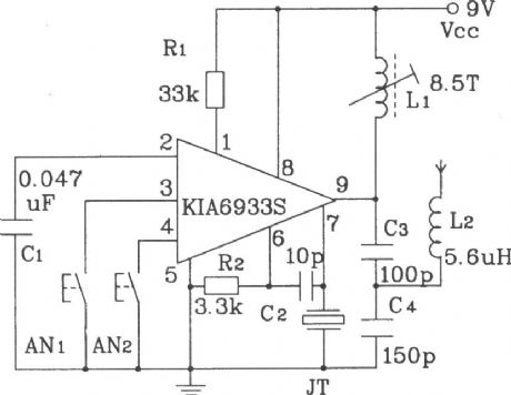
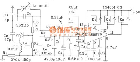
The internal RF remote control transmitter KIA6933S is composed of pulse generator within the integrated circuit KIA6933S, the duty factor regulator, mixer, oscillator and RF carrier frequency amplifier. The remote control transmitter circuit composed of it hasmany features, such assimpleexternal rotation circuit, easy to debugging. Usually 4 states remote controls can be achieved. The internal KIA6957P receiving circuit has two low-frequency amplification units, integration circuit and signal comparison detection circuit. Since there is not high-frequency receiving circuit, it uses high-frequency super-regenerative receiver circuit. The similar types of circuits are: DF-27/DJ-27, TA7333P/TA7657P.
(View)
View full Circuit Diagram | Comments | Reading(2619)
4096 single-function remote control transmitter, receiver application circuit composed of KD-12E/KD-12F
Published:2011/10/17 21:35:00 Author:Rebekka | Keyword: single-function , remote control , transmitter and receiver
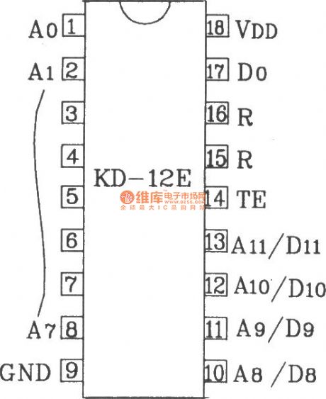

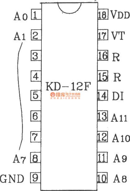
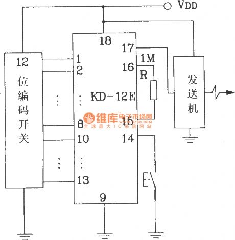
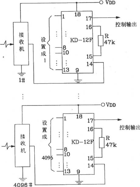
KD-12E/KD-1290 transistor devices are made in the factory in Zhejiang, Xiaoshan for the latest remote control, telemetry dedicated encoding / decoding ICs. This circuit can simplify many complex remote control system and circuit detection system. It is a high reliability circuit. The current device has been widely used in home appliances, industrial control, alarm and robot control.
Electrical parameters: Since KD-12E and KD-12D (F) use CMOS process, therefore it has a wide operating voltage range, low power consumption. The typical operating voltage range is 2 ~ 5V, quiescent current (no oscillations) is 0.1 ~ 1μA. As A8/D8 ~ A11/D11 is used to control code input, each 256 code can have 16 seeds passwords. It can be completed by artificially setting different control functions.
(View)
View full Circuit Diagram | Comments | Reading(1599)
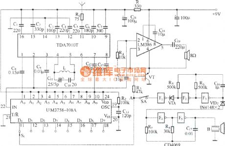
Small wireless call system circuit diagram (BA1401/TDA7010T)
Published:2011/10/18 2:07:00 Author:Rebekka | Keyword: Small wireless call system
View full Circuit Diagram | Comments | Reading(2966)
SA9615 FSK Decoding IC diagram
Published:2011/9/13 2:28:00 Author:Rebekka | Keyword: FSK Decoding
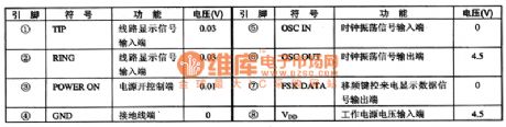
SA9615 is a shift frequency keying decoder integrated circuit. It is widely used for receiving, displaying the calling number sent by switching equipment and information products(such as caller ID cordless, corded telephones, etc.).1. Pin functions and data.SA9615 integrated circuit uses 8-pin dual package structure, the pin functions and data of the integrated circuit are listed in table 1.2. Signal flow.The main signal inputs from ①, ② pin. The demodulated information outputs from pin ⑦ in serial. It will be sent to single-chip microcomputer. And it will be dealed by microcomputer and sent to the desplay. The information will be stored at the same time. (View)
View full Circuit Diagram | Comments | Reading(1671)
LM909 radio telecontrol receiving decoding circuit diagram
Published:2011/10/16 22:20:00 Author:Ecco | Keyword: radio telecontrol, receiving decoding
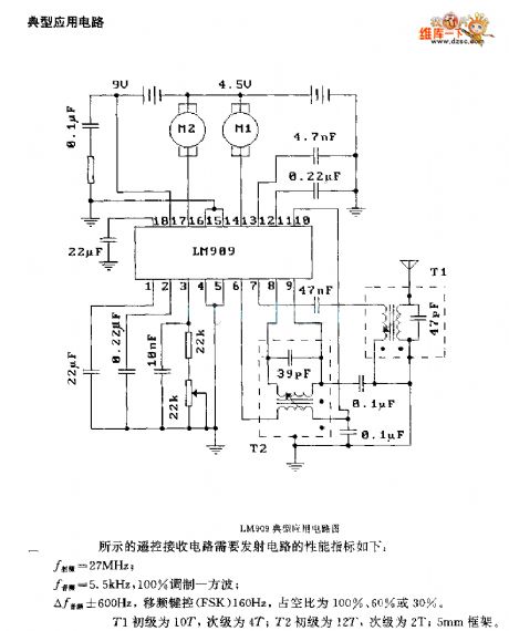
The telecontrol receiving decoding circuit's performance index shown as the chart are as follow: f radio frequency =27MHz, f audio frequency =5.5KHz, 100% modulation - square-wave; f radio frequency=±600Hz, and the frequency shift keying (FSK) is 160Hz, and the dutyfactor is 100%, 60% or 30%, T1's primary is 10T, secondary is 4T; T2's primary is 12T, secondary is 2T; the frame is 5mm.
(View)
View full Circuit Diagram | Comments | Reading(2352)
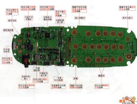
Motorola 2000 cell phone material object maintaining diagram
Published:2011/10/17 1:33:00 Author:Ecco | Keyword: Motorola , cell phone, material object , maintaining diagram
View full Circuit Diagram | Comments | Reading(3150)
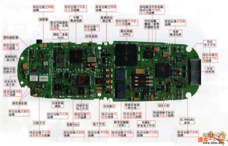
Eastcom EL610 cell phone board circuit diagram
Published:2011/10/17 1:14:00 Author:Ecco | Keyword: Eastcom , cell phone board
View full Circuit Diagram | Comments | Reading(1793)
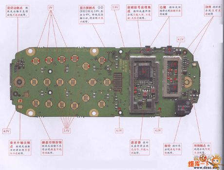
Bird S1000 cellphone repairing diagram 1
Published:2011/10/16 21:37:00 Author:Ecco | Keyword: Bird, cellphone repairing
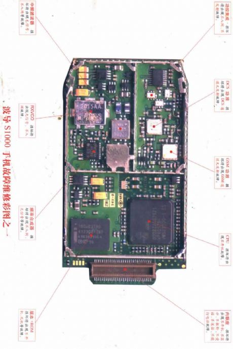
View full Circuit Diagram | Comments | Reading(1150)
485 and 75176 communications circuit diagram
Published:2011/9/15 1:53:00 Author:Rebekka | Keyword: communications circuit
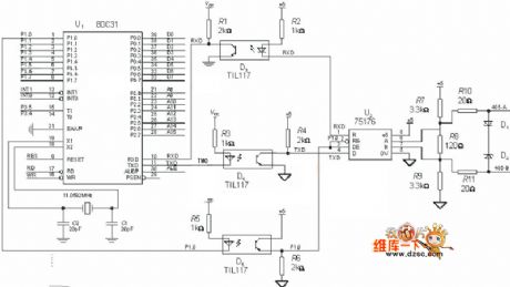
View full Circuit Diagram | Comments | Reading(12752)
| Pages:5/32 1234567891011121314151617181920Under 20 |
Circuit Categories
power supply circuit
Amplifier Circuit
Basic Circuit
LED and Light Circuit
Sensor Circuit
Signal Processing
Electrical Equipment Circuit
Control Circuit
Remote Control Circuit
A/D-D/A Converter Circuit
Audio Circuit
Measuring and Test Circuit
Communication Circuit
Computer-Related Circuit
555 Circuit
Automotive Circuit
Repairing Circuit