
Communication Circuit
Index 8
300_BAUD_BIT_BOFFER_RECEIVER
Published:2009/7/14 7:37:00 Author:May
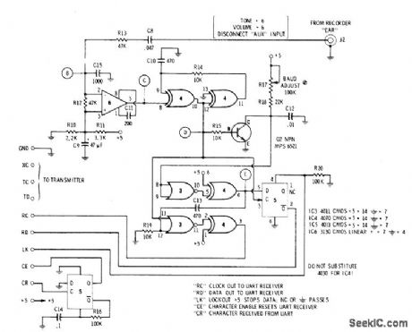
Used with ordinary cassette recorder to convert half sine waves of recorded serial data to corresponding digital 1s and 0s. Output of recorder passes through filter and limiter IC6 to give square wave at point C whose zero crossings correspond to recorded sine wave. Leading and trailing edges of square wave are converted to narrow positive pulses by EXCLUSIVE-OR gate IC4 to give stream of pulses at D, one for each zero crossing. Transistor circuit forms retriggerable mono that is adjusted so point E goes positive three-fourths of way through low-frequency (1200 Hz) half-cycle. Point E then has stream of eight pulses for 0 and no pulses for 1. Final flip-flop provides recovery of data as is and 0s. Leading edge of waveform at D is shortened and combined with clock pulses to provide composite UART clock output. Boffer system eliminates errors commonly encountered when attempting to record square waves on tape with low-cost recorder.-D. Lancaster, TV Typewriter Cookbook, Howard VV. Sams, Indianapolis, IN, 1976, p 167-171. (View)
View full Circuit Diagram | Comments | Reading(1653)
SYNCHRONOUS_VIDEO_DETECTOR
Published:2009/7/15 3:34:00 Author:Jessie
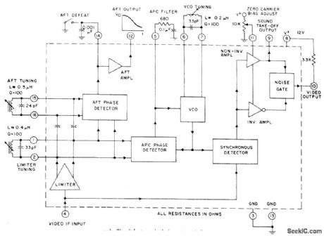
RCA CA3136E serves as video IF PLL synchronous detector for color TV receivers. Phase-locked oscillator demodulates 45.75-MHz video IF signals. Circuit features include automatic fine tuning voltage (AFT) for DC control of tuner, adjustment of zero-carrier DC level at video output terminal, amplifier arrangement for inverting noise impulses toward black level, and separate noninverting output terminal for sound IF. Re-quires single 12-V supply.- Linear Integrated Circuits and MOS/FET's, RCA Solid State Division, Somerville, NJ, 1977, p 374. (View)
View full Circuit Diagram | Comments | Reading(1830)
SSTV_VERTICAL_SYNC_INDICATOR
Published:2009/7/15 3:24:00 Author:Jessie
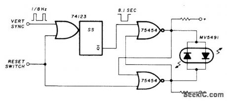
Retriggerable mono MVBR using SN74123 is triggered by 0.125-Hz vertical sync pulse of amateur television system. Absence of pulse allows mono to time out and change state of LED from green to red. Vertical reset switch must then be used to p restart vertical sweep and reset LED. Uses Monsanto MV5491 dual red/green LED, with 220 ohms in upper lead to +5 V supply and 100 ohms in lower +5 V lead because red and green LEDs in parallel back-to-back have different voltage requirements. Drivers for LEDs are SN75454.-K. Powell, Novel Indicator Circuit, Ham Radio, April 1977, p 60-63. (View)
View full Circuit Diagram | Comments | Reading(1187)
INFRARED_DATA_TRANSMITTER
Published:2009/7/14 8:27:00 Author:May
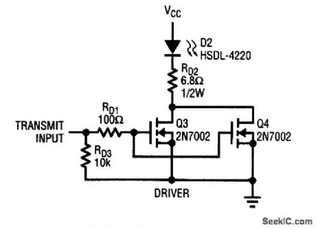
This figure shows anIrDA transmitter. (View)
View full Circuit Diagram | Comments | Reading(2011)
PHOTOTRANSISTOR_IR_RECEIVER
Published:2009/7/14 8:26:00 Author:May
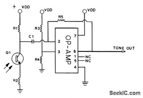
This receiver uses an op amp and a phototransistor as a recetver for IR signals. Q1 is a phototransistor. The op amp is CMOS or FET, such as a TL081, etc. R1 and R2 depend on phototransistor, but are typically 2.2 kΩ and 330Ω, respectively. R3=R4=10 kΩ, R5=100 kΩ, and C1 is 0.1 μF (or larger ). (View)
View full Circuit Diagram | Comments | Reading(2749)
SSTV_DEFLECTION_DRIVE
Published:2009/7/15 2:55:00 Author:Jessie
Developed for use in line time-base amplifier of 4-Hz slow-scan TV system. Emitter-follower in driver stage is used with first transistor to match output impedance of UJT sawtooth oscillator. Will drive deflection coils of 17-ineh CRT (coil resistance about 5 ohms).-M. Hadley, Deflection Coil Driver for Slow-Scan Television, Wireless World, March 1974, p. 18. (View)
View full Circuit Diagram | Comments | Reading(3325)
AF_PHASE_SHIFTER
Published:2009/7/15 2:54:00 Author:Jessie
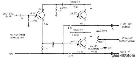
Developed for testing chroma demodulator in color TV receiver. Audio oscillator is used as source of sine waves. First stage is phase inverter, followed by two emitter-followers. Resulting output signals of opposite phase are combined through a small capacitor (0.022μF, selected for frequency used) from one channel and 50K variable resistor from other channel. 90°phases are judged by position of sine waves on screen of CRO; 90° is halfway between 0° and 180°.-C. Babcoke, Waveforms Explain Chroma Demodulators, Electronic Servicing, Sept. 1972, p 22-23, 26-28, and 30. (View)
View full Circuit Diagram | Comments | Reading(1129)
CRYSTAIVFO_SYNC_GENERATOR
Published:2009/7/15 2:52:00 Author:Jessie
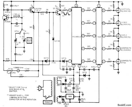
With crystal, can be used as system sync generator or as drive for staircase generators, custom pattern generators, and special TV test equipment. When VFO-controlled, circuit provides variable-frequency sync needed for determining pull-in range of sweep oscillators in TV sets and VTR decks. Clock-pulse section uses Q1 and Q2 as 1.00800-MHz Butler oscillator. On VFO operation, oscillator frequency can be varied ±3.5% from mean. Sine-wave output of Q2 is converted to square wave by Q3 for application to clock input of Hughes HSUB0525 sync generator. Each output of sync generator feeds one of inverters in 7404, providing 3.3 V P-P signal into 75-ohm load for each output.-M. J. Salvati, VFO Adds Versatility to TV Sync Generator, EDN Magazine, May 20, 1974, p 70 and 72. (View)
View full Circuit Diagram | Comments | Reading(2756)
IR_REMOTE_CONTROL_RECEIVER_1
Published:2009/7/14 11:11:00 Author:May
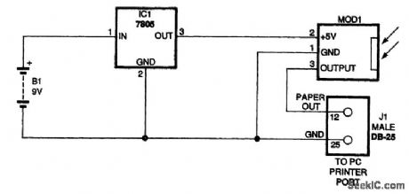
The figure shows a schematic of the IR receiver circuit. The heart of the circuit is MOD1, an infrared detector module that removes the IR carrier frequency and transmits only the data that are encoded in the received IR signal. A suitable IR module is available at Radio Shack (No. 276-137).The IR module needs a clean 5-V power supply, which is provided by IC1, a 7805 regulator. Power is supplied to the regulator by 9-V battery B1. The output of the module is wired to a male DB-25 multipin connector. The infrared detector module receives a signal, filters it, and removes the 40-kHz carrier. The output of the module is a TTL-level signal consisting of long and short pulses. The PC records those voltage levels over time, while the signal is being sent, and stores the data in a file. The line normally used by the PC's printer port to indicate that the printer is out of paper (pin 12) is used in this project to accept data from the IR module. The I/O port is located at the address ox379. Bit 5 corresponds to input pin 12. Various software programs are required to let a PC store information input to its printer port. (All of the software is available on the Gernsback BBS-516-293-2283, v.32, v.42bis-contained in a file called IR-TEST.ZIP.) The source code of the first program, IRLOG.EXE, is written in C. The program stores the value it reads from the PC's printer port into an array. When the input line is logic high, the ASCII character 1 is stored in the array. When the input line is logic low, ASCII character 0 is stored. (View)
View full Circuit Diagram | Comments | Reading(1378)
IR_REMOTE_CONTROL_RECEIVER
Published:2009/7/14 8:16:00 Author:May
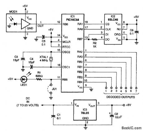
A schematic diagram of the remote-control receiver is shown. The heart of the circuit is IC1, a PIC16C54 8-bit CMOS manufactured by Microchip. The microcontroller stores its data in IC2, a 93LC46 1-kbit serial EEPROM (electrically erasable programmable read-only ntemory), also manufactured by Microchip. In this application, the 93LC46 has a three-line interface with the microcontroller. The three lines are CHIP SELECT, CLOCK, and DATA IN/OUT. Because DATA IN and DATA OUT share the same line, a resistor (R2)limits the current flow during transitions between writing and reading when there are conflicting logic levels. The microcontroller communicates with the 93LC46 by placing a logic high on the CHIP SELECT pin. Data are then transferred serially to and from the 93LC46 on the positive transition of the CLOCK line. Each read or write function is preceded by a start bit, an opcode identifying the function to be performed (read, write, etc.), then a 7-bit address; this is followed by the 8 bits of data which are being written to or read from that address. Immediately preceding and following all write operations, the microcontroller sends instructions to the 93LC46, which enables or disables the write function, thereby protecting the data that have been stored. In the programming mode, IC1 reads an IR data stream from MOD1 and converts it to data patterns that can be stored in IC2. These data patterns are held for comparison while the unit is in normal operation. Power for the circuit is conditioned by IC3, a 78L05 low-current, 5-V regulator, which will accept any dc input voltage between 7 and 25 V. Capacitors C1 and C2 stabilize the operation of the regulator. Crystal XTAL1 sets the internal oscillator of IC1 to 4 MHz. Jumper JU1 consists of two closely spaced pads on the PC board that, when momentarily jumpered with a screwdriver or other piece of metal, places IC1 in the programming mode and lights LED1. The source and object code are available on the Gernsback BBS (516-293-2283, v.32, v.42bis) as a file called IREC.ZIP for those who wish to program their own PICs and have the proper equipment to do so. (View)
View full Circuit Diagram | Comments | Reading(5760)
300_BAUD_BIT_BOFFER_TRANSMITTER
Published:2009/7/14 6:54:00 Author:May
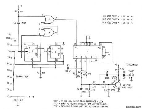
Permits recording of serial data on ordinary Iow-cost cassette tape recorders for bulk storage of data to be used later in microprocessor. Requires 19,200-Hz reference input to terminal XC from external clock. Feedback from sine-wave synthesizer IC1 to dividby-4 counter IC2 automatically synchronizes system so sine waves automatically switch just before zero crossing each time serial data changes from 1 to 0 or back again. Output consists of 16 half sine waves at 2400 Hz for mark or digital 1 and 8 half sine waves at 1200 Hz for space or digital 0, for feed to input of cassette recorder. Circuit eliminates errors commonly encountered when attempting to record square waves on tape with low-cost recorder.-D. Lancaster, TV Typewriter Cookbook, Howard W. Sams, Indianapolis, IN, 1976, p 167-171. (View)
View full Circuit Diagram | Comments | Reading(2109)
INFRARED_ALARM_RECEIVER
Published:2009/7/14 7:33:00 Author:May
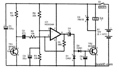
The full circuit diagram for the infrared receiver is given here. TR1 is a phototransistor, and it is used in a common-emitter amplifier. However, no bias current is fed to the base (b) terrrtinal of TR1.The collector (c) current is governed by the light level received by TR1. The higher the received light level, the higher the current flow. The pulses of infrared from the transmitter therefore produce pulses of leakage current through TR1, which give small negative pulses at TR1's collector. The output signal for TR1's collector is coupled by capacitor C2 to a high-gain inverting amplifier based on IC1. Resistors R2 and R5 ire the negative-feedback network, and these set the closed-loop voltage gain of IC1 at 220 times. Capacitor C4 couples the amplified output signal from IC1 pin 6 to a conventional half-wave rectifier and smoothing circuit (D1, D2, and C5). Germanium, rather than silicon, diodes are used in the rectifier, because germanium types have a lower forward voltage drop.This gives slightly improved sensitivity. The positive dc signal developed across capacitor C5 drives the base of TR2, which is a simple common-emitter switch that controls the relay RLA coil. (View)
View full Circuit Diagram | Comments | Reading(2717)
MONO_CORDLESS_HEADPHONE_IR_TRANSMITTER
Published:2009/7/14 7:30:00 Author:May
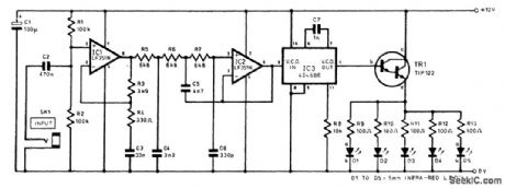
The preemphasis is applied by IC1, which is basically just an op amp used in the noninverting mode. At low and middle frequencies, the impedance of capacitor C3 is high in relation to the resistance of R3. Consequently, there is virtually 100 percent negative feedback through resistor R3, and IC1 has a closed-loop gain of little more than unity. At higher frequencies, the impedance of C3 is relatively low, and a significant proportion of the feedback through R3 is decoupled. This gives a closed-loop voltage gain that steadily rises with increased input frequency, with almost 20 dB of gain being provided at the highest audio frequencies. Resistor R4 limits the closed-loop voltage gain of IC1 at frequencies above the audio range. The low-pass filter is a conventional third-order (18 dB/octave) type based on IC2. This filter gives fractionally less than the full 20-kHz audio bandwidth, but does not significantly impair the quality of the input signal. A CMOS “micropower” PLL is used for IC3, but, in this circuit, only the VCO stage is utilized. No connections are made to any of the other sections of IC3. The output of IC2 is direct-coupled to the control input of the VCO (IC3 pin 9). Capacitor C7 and resistor R8 are the VCO timing components, and they set the center frequency at roughly 100 kHz. Transistor TR1 is a high-gain power Darlington device, which is used here as an emitter-follower buffer stage. This can easily source the 500-mA ON current of the LEDs. A bank of five LEDs is used, and each one has a separate current-limiting resistor (R9 to R13). (View)
View full Circuit Diagram | Comments | Reading(1733)
INFRARED_ALARM_TRANSMITTER
Published:2009/7/14 7:28:00 Author:May
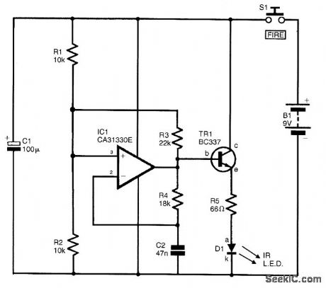
The circuit diagram for the infrared transmitter appears in this figure. The oscillator uses IC1 as a relaxation oscillator. Capacitor C2 and resistor R4 are the timing components, and they are connected between the output of IC1 and its inverting input (pin 2). A roughly square-wave signal is generated at pin 6, the output of IC1. This signal is used to drive infrared LED D1, via emitter-follower buffer-stage transistor TR1 and current-limiter resistor R5. The specified value for R5 sets the LED current at nearly 100 mA, but as the LED is switched off for about 50 percent of the time, the average LED current is a little under 50 mA. This is the maximum acceptable drive current for most normal infrared LEDs. (View)
View full Circuit Diagram | Comments | Reading(1488)
WARBLE_TONE_INFRARED_TRANSMITTER
Published:2009/7/14 7:23:00 Author:May
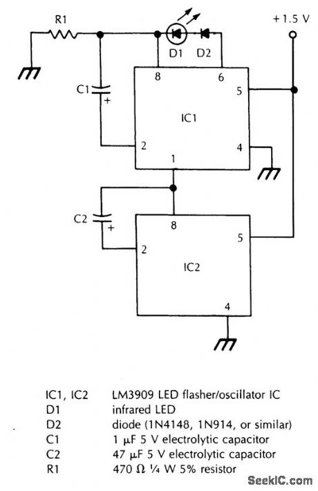
IC1 and IC2 are LM3909 LED flasher-oscillator devices. IC2 generates a low-frequency square wave that modulates the frequency of IC1. This circuit is useful for IR testing, communications link signal source, etc. (View)
View full Circuit Diagram | Comments | Reading(1057)
DTMF_INFRARED_TRANSMITTER
Published:2009/7/14 7:21:00 Author:May
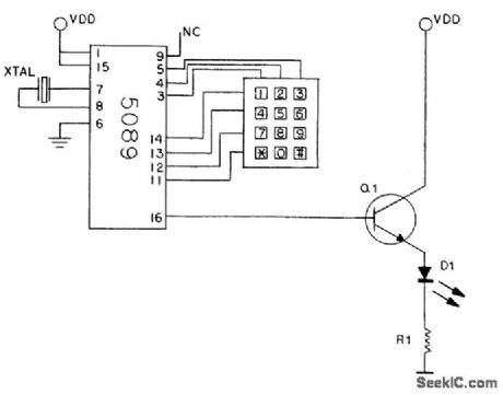
This transmitter uses a 5089 DTMF generator chip and a keypad to generate DTMF signals and modulate them on an IR light beam from an IR LED. Xtal is a 3.579-MHz TV burst crystal. (View)
View full Circuit Diagram | Comments | Reading(5986)
UPWARD_SHIFT_RTTY_DEMODULATOR
Published:2009/7/15 2:21:00 Author:Jessie
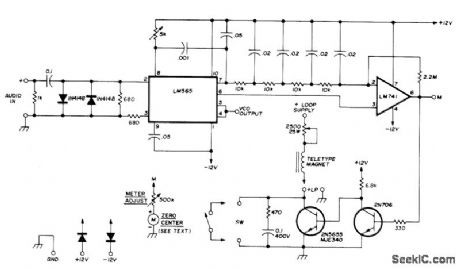
PLL demodulator serves for copying AFSK/FSK up-ward-shift RTTY signals, 2N706 switches 2N5655 on and off, reversing polarity of voltage from LM741 comparator on mark/hold as needed for smooth upward-shift copy. Works equally well on wide-shift or narrow-shift signals. Zero-center tuning meter will show full-scale minus (left) reading on mark/hold signal Meter may not be needed on AFSK.-N. Stinnette, Update of the Phase-Locked Loop RTTY Demodulator, Ham Radio, Aug. 1976, p 16-17.
(View)
View full Circuit Diagram | Comments | Reading(2727)
FSK_DEMODULATOR_1
Published:2009/7/15 2:19:00 Author:Jessie

Uses IC originally developed for stereo multiplex decoders, containing phase-locked loop suitable for demodulating teleprinter FSK signals. Circuit shown requires only small input signal for phase lock, gives visual indication with lamp when phase lock has occurred, and requires only pair of 2N3055 drive transistors between outputs A-B and teleprinter receiving solenoids. Article also gives this output circuit and setup procedure.-K S. Beddoe, Teleprinter Terminal Unit Uses Phase-Locked Loop, Wireless World, Dec. 1973, p 605. (View)
View full Circuit Diagram | Comments | Reading(2277)
RAM_FOR_RTTY
Published:2009/7/15 2:14:00 Author:Jessie
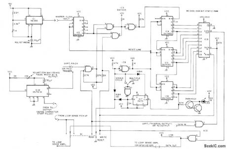
Erasable MC2102 1024-bit RAM stores two Teletype lines (128 characters) of Baudot code for readout at machine speed Can also serve in place of tape loop for frequently used code messages such as CQ calls. Values shown with IC1 timer are for 728-Hz master clock (16× 45.45 bauds). Stored message is volatile, disappearing when power is turned off. For permanent storage, use ROM in place of RAM.-H. P. Fischer, RTTY Scratchpad Memory, 73 Magazine, June 1977, p 54-55. (View)
View full Circuit Diagram | Comments | Reading(1923)
COAX_DRIVER_AND_RECEIVER
Published:2009/7/14 4:41:00 Author:May
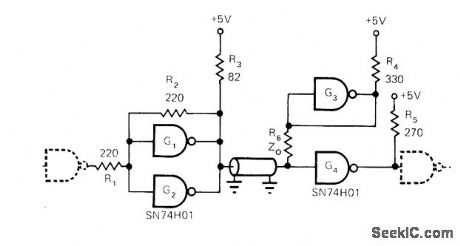
Uses two TTL gates of SN74H01 package to form either driver or receiver for transmitting data over RG59 or RG174 coax at rates exceeding 10 megabits per second, with distance increasing from 400 meters at 10 Mb/s to over 1000 meters at 100 kb/s for RG59 and lesser distances for RG174. Can also be used for twisted-pair lines but at lower data rates. Bias gate G3 exhibits low output impedance, for terminating channel load resistor R6.-R. W. Stewart, Two TTL Gates Drive Very Long Coax Lines, EDN Magazine, Oct, 1, 1972,p49. (View)
View full Circuit Diagram | Comments | Reading(1233)
| Pages:8/32 1234567891011121314151617181920Under 20 |
Circuit Categories
power supply circuit
Amplifier Circuit
Basic Circuit
LED and Light Circuit
Sensor Circuit
Signal Processing
Electrical Equipment Circuit
Control Circuit
Remote Control Circuit
A/D-D/A Converter Circuit
Audio Circuit
Measuring and Test Circuit
Communication Circuit
Computer-Related Circuit
555 Circuit
Automotive Circuit
Repairing Circuit