
Communication Circuit
Index 12
WIRELESS_FM_CODE_PRACTICE_TRANSMITTER
Published:2009/7/12 20:45:00 Author:May
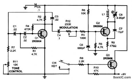
The circuit shown is a low-power, tone-modulated FM transmitter that can be used with any FM broadcast receiver for code practice. Transistor Q1 and its associated components make up a phaseshift audio-frequency generator circuit. Potentiometer R11 sets the tone frequency. Transistor Q2 is connected in a high-frequency RE oscillator circuit that operates in the FM broadcast band. Potentiometer R12 sets the modulation level. Transistor Q3 operates as a switch, turning on the FM transmitter each time the CW key is closed. Coil L1 is a homemade air-wound coil. Take a 6 1/2-in length of 20-gauge enamel-covered wire and close-wind it around a 1/4-in-diameter form; leave about 1/4 in free at each end. Remove the insulation from the ends and slide the coil off the form. The overall length of the finished coil should be about 1/4 in. Set R11 and R12 to midposition and close the CW key. Then set your FM receiver to a clear spot on the low end of the dial and slowly adjust C8. Once the tone is heard, R11 can be set for the desired tone frequency and the tone level set by R12. If your oscillator won't tune to the top end of the band, carefully stretch the windings of L1 and retune. The circuit's operating range can be increased by adding a very short antenna to the emitter of Q2. (View)
View full Circuit Diagram | Comments | Reading(2660)
TYPEWRITER_KEYS_CW_TRANSMITTTER
Published:2009/7/11 3:47:00 Author:May
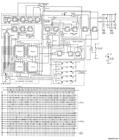
Allows operator to send perfect Morse code simply by typing messages on alphameric keyboard. Accuracy is determined only by typing skill of operator. One RC oscillator controls mark-space ratio of Morse characters and duration of character and word spaces, while clock oscillator is divided down and switched to give sendingspeed choices of 6, 12, 24, and 48 words per minute. Each square on keyboard diagram is SPST switch, and each cross at intersection issilicon switching diode such as 1N914. 0utputs of keyboard switches are converted into 15-bit code for feeding into 64-character first-in first-out memory using four MP3812B ICs for storage and for generating corresponding Morse characters. Article gives construction and adjustment details.-C. I. B. Trusson, Morse Keyboard and Memory, Wireless World, Jan. 1977, p 55-59. (View)
View full Circuit Diagram | Comments | Reading(1473)
TRANSISTOR_PIN_FINDER
Published:2009/7/11 2:29:00 Author:May
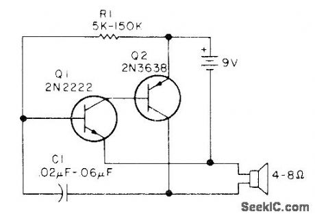
Simple audio oscillator is assembled as shown and values of R1 and C1 adiusted for desired tone. General-purpose transistor to be tested is then substituted in circuit (NPN for Q1 or PNP for Q2) and rotated in socket until oscillator works again; pins then correspond to those of the good transistor. If oscillator will not work in any of three possible positions, transistor under test is bad.-Circuits, 73 Magazine, July 1977, p 34. (View)
View full Circuit Diagram | Comments | Reading(4040)
LOW_COST_BEACON_TRANSMITTER
Published:2009/7/11 2:01:00 Author:May

This transmitter uses a 48-MHz crystal oscillator to drive a diode tripler to the 144-MHz amplifier. The output is 5 to 10 mW. (View)
View full Circuit Diagram | Comments | Reading(1971)
5_W_80_m_CW_TRANSCEIVER
Published:2009/7/11 1:58:00 Author:May
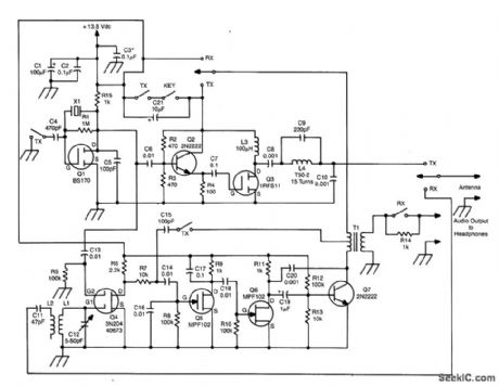
This transceiver has a 3-stage transmitter and a direct-conversion receiver. Q1 is the transmitter's oscillator, and the frequency is controlled by X1, which also serves as the receiver local oscillator. Buffer Q2 drives final amplifier Q3 to about 5 W output. The B+ lead to these stages is keyed. The receiver consists of mixer Q4 followed by high gain amplifiers Q5/Q6/Q7. The audio signal appears at the secondary of Q7. In the transmit mode, Q5/Q6/Q7 serve as a sidetone oscillator. A 6PDT switch is required for the T/R switching. (View)
View full Circuit Diagram | Comments | Reading(1768)
HF_LOW_POWER_CW_TRANSMITTER
Published:2009/7/11 1:54:00 Author:May
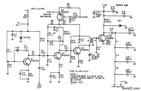
Suitable for amateur use, this 1.5-W transmitter runs on a 12-V supply. Q1 is an oscillator using a surplus FT243 crystal. Q2 is a buffer driver and is keyed via keying transistor Q5. Q3 acts as a driver for Q4 (which should be heatsinked). Q4 develops about 1.5-W output. Coil data is given in the parts list. C12 is adjusted for best power output. (View)
View full Circuit Diagram | Comments | Reading(1336)
2_m_TRANSMITTER
Published:2009/7/11 1:40:00 Author:May
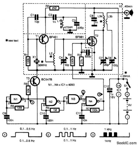
The transmitter was designed specifically for use by radio amateurs as a radio beacon. As such, it provides a good-quality signal that is free of unwanted harmonics.Transistor T1, in association with crystal X1, operates as a 36-MHz oscillator. Filter L1/C3 obviates any tendency of the circuit to oscillate at 12 MHz (the fundamental frequency of the crystal).Circuit L2/C4 is tuned to the fourth harmonic of the oscillator signal (144 MHz). This signal is fed to the aerial via a buffer stage that consists of T2, a double-gated FET. The (amplitude) modulating signal is applied to the second gate of the buffer. The output power of the transmitter has been kept low, about 10 to 40 mW.The modulating signal is generated by N1, an oscillator that switches the transmitter on and off via transistor T3. The switching rate lies between 0.1 and 0.5 Hz. When the output of N1 is low, T3 is switched off, and the transmitter is inoperative because the supply is disabled. When the output of N1 is high, T3 is on and the transmitter operates normally.The digital pattern at the gate of T2 shapes the modulating signal. Gate N2 generates a square wave at afrequency of0.1 to 1 Hz. As long as the output of T3 is high, N4 oscillates atafrequency ofabout 1 kHz. At the relevant gate of N2, there is, therefore, a periodic burst-signal at 1 kHz, and this signal is used to modulate the transmitter.The digital pattern at the relevant gate of T2 can be varied to individual requirements by altering the values of the feedback resistors in the digital chain. The transmitter is calibrated by setting trimmers C4, C7, and C8 for maximum output power.Inductors L2 and L3 are wound from 0.8-mm diameter enamelled copper wire: L2 =5 turns with a tap of 1 turn from ground; L3A=3 turns and L3B=2 turns. The coupling between L3A and L3B should be arranged for maximum output power. The circuit draws a current of only 20 mA, which enables the trans-mitter to be operated from a 9-Y battery for several hours. (View)
View full Circuit Diagram | Comments | Reading(1875)
AMATEUR_TELEVISION_TRANSMITTER
Published:2009/7/11 1:37:00 Author:May
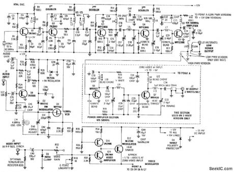
Although the unit was designed for 2 W operation, Q6 and Q7 stages and associated components can be omitted and about 1 to 30 mW of RE can be obtained by link coupling to L9. A complete set of parts, including PC board is available from North Country Radio, P.O.Box 53, Wykagyl Station, New Rochelle, NY 10804. (View)
View full Circuit Diagram | Comments | Reading(1939)
LOW_POWER_HF_TRANSMITTER
Published:2009/7/11 1:28:00 Author:May
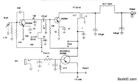
This transmitter runs up to 1/2W on the 40-m amateur band. Coils are wound on T25 and FT23 toroids, respectively. Point A is connected to point B to key the oscillator, along with the ftnal (point C) to leave the oscillator running constantly. Use 1/10-W resistors and VERY small components. (View)
View full Circuit Diagram | Comments | Reading(1780)
20_m_CW_TRANSCEIVER
Published:2009/7/11 1:26:00 Author:May
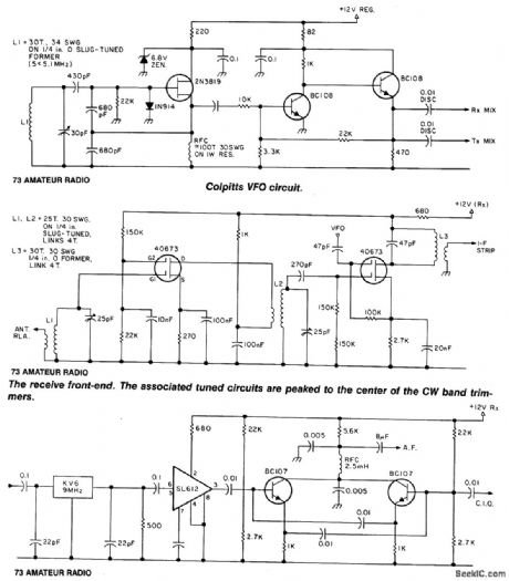
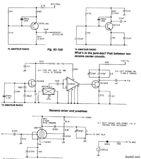
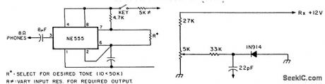
The Colpitts VFO circuit (Fig. 93-1(a)) has gate clamping to improve stability. It is followed by two buffers: the second provides individual outputs to the transmitter and receiver. An RIT circuit operates on receive. The front end uses 40673 dual-gate MOSFETs (Fig. 93-1(b)). The tuned circuits are peaked to the center of the CW band with the trimmer. The mixer output is link-coupled to a KVG 9-MHz SSB filter whose output is amplified by an SL612 IF amplifier IC (Fig. 93-1(c)).The product detector uses two BC107 transistors. Carrier reinjection is from a crystal oscillator using the USB crystal supplied with the KVG filter. Figure 93-1(d) and 93-1(e) contain: an FET oscillator and a pnp bipolar oscillator. Use either or alter the circuit polarities to suit an npn transistor. The transmitter mixer is an MD108 (Fig. 93-1(f)), fed from the VFO and the LSB carrier-injection oscillator.A simple diode/meter circuit measures the relative power output (Fig. 93-1(g)). Sidetone is provided by an NE555 circuit (Fig. 93-1(h)). (View)
View full Circuit Diagram | Comments | Reading(2202)
V_F_CONVERTER_FOR_TRANSDUCER
Published:2009/7/10 23:27:00 Author:May
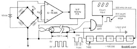
Output of low-level transducer such as temperature bridge can be transmitted reliably over long wires (100feet or more) in serial form if changes in 100-ohm resistive thermal device (RTD) are converted to corresponding changes in frelquency with almost any commercially available V/F converter, Typical converter has 0-10 V fullscale analog input and 0-10 kHz output. If 5 V is applied to input, output pulse train will have rate of 5 kHz ±0.5 Hz, which can be counted for 1 s or less and displayed on digital readout to show analog value Instrument amplifier can be Datel AM201 or equlvaient.-E. L. Murphy,Sending Transducers Signals over 100 Feet?,Instuments Control & Systems,June 1976,p 35-39. (View)
View full Circuit Diagram | Comments | Reading(1068)
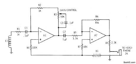
ACOUSTIC_SOUND_RECEIVER
Published:2009/7/10 21:13:00 Author:May
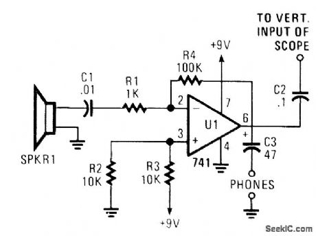
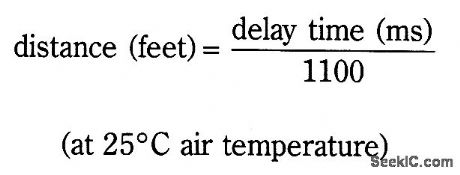
The receiver is an audio amplifter fed by SPKR1, a piezo speaker that is used as a microphone. A scope or headphones can be used as a detector. The scope can be triggered horizontally by the transmitted acoustic pulse; the vertical display can be used to drive the delay time, and hence the distance.
(View)
View full Circuit Diagram | Comments | Reading(1371)
ACOUSTIC_SOUND_TRANSMITTER
Published:2009/7/10 21:10:00 Author:May
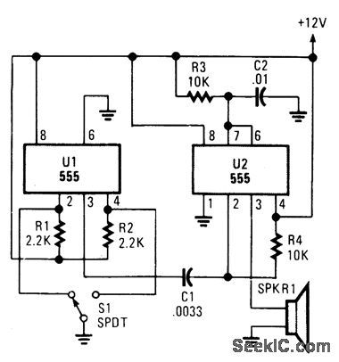
Pulsed sound is produced by this circuit. U1 is used as a bistable multivibrator, which acts as a contact debouncer for S1. C1 feeds a trigger pulse to U2, which feeds apulse to SPKR1, to piezo transducer.Values are shown for a pulse width of 110 μs. (View)
View full Circuit Diagram | Comments | Reading(1185)
SINGLE_IC_WITH_TRANSFORMERS
Published:2009/7/10 5:14:00 Author:May
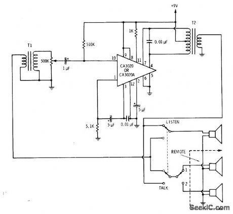
CA3020 differential amplifier uses AF input transformer T1 to matchloudspeakers(used as microphone) to higherinput resistance of IC,AF outputtransformer T2 similarly matches IC to loudspeakers operating conventionally.-E. M. Noll, Linear IC Principles, Experiments, and Projects, Howard W. Sams,Indianapolis,IN, 1974, p 100-101. (View)
View full Circuit Diagram | Comments | Reading(1010)
AUDIO_INDUCTION_RECEIVE
Published:2009/7/10 4:43:00 Author:May
Used to pick up audio signal being fed to low-impedance single-wire loop encircling room or other area to be covered. Pickup loop L1 is 100-500 turns wound around plastic case of receiver. Opamp sections are from Motorola MC3401P or National LM3900 quad opamp. Supply can be 9-15 V. Requires no FCC license. Can be used as private paging system if audio amplifier of transmitter has microphone input.-C. D. Rakes, Integrated Circuit Projects, Howard W. Sams, Indianapolis, IN, 1975, p 23-25. (View)
View full Circuit Diagram | Comments | Reading(1577)
PROJECTILE_ACCELERATION_TELEMETER
Published:2009/7/19 22:27:00 Author:Jessie
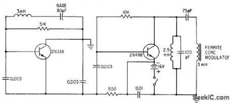
Microwave signal at 24,000 Mc is aimed down barrel of howitzer by sheet aluminum reflector that is replaced abet each firing. Variations in reflection coefficient of ferrite device on projectile nose modulate reflected micro-wave signal from moving projectile, at frequency dependent on acceleration. Circuit shows encapsulated transducer mounted on nose. Capacitance gage produces frequency shift of 70-kc subcarrier that is proportional to acceleration, for driving ferrite-core modulator through amplifier stage.-W. M. Kendrick and L. A. Peters, Projectile Telemetry with Microwaves, Electronics, 33;38, p 68-71.
(View)
View full Circuit Diagram | Comments | Reading(1102)
MICRO_MULTIPLEXER
Published:2009/7/19 22:24:00 Author:Jessie
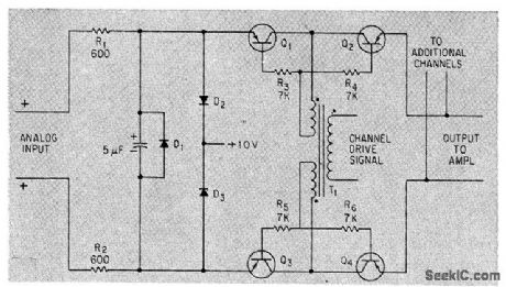
Solid-state high speed time-division commutator connects several low-level inputs, one at a time, to common differential bus. Each multiplexor channel consists of two transistor switch pairs.-J. V. Dirocco und J. W. Peghiny, Low-Level Encoding Approach: Latest Details of Titan II Telemetry, Electron'Ics, 35:47, p 36-39. (View)
View full Circuit Diagram | Comments | Reading(906)
BASIC_SCALER
Published:2009/7/19 22:23:00 Author:Jessie
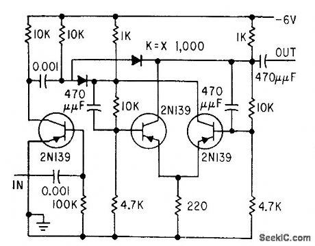
Each staler stage is bistable circuit with trigger amplifiers between each pair of stages. Used to make 512 counts from ion chamber give one output to telemetry system.-D. Enemark, Balloon-Borne Circuits Sort High-Altiiude Cosmic Rays, Electronics, 32:35, p 52-55. (View)
View full Circuit Diagram | Comments | Reading(1307)
60_MW_TRANSMITTER
Published:2009/7/19 22:23:00 Author:Jessie
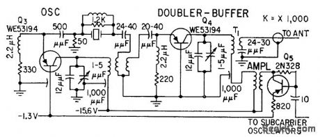
Amplitude modulation is applied at collector of amplifier-doublet Q4.-H. L. Richter et al., Instrumehting the Explorer I Satellite, Electronics, 32:6, p39-43. (View)
View full Circuit Diagram | Comments | Reading(1126)
F_M_MODULATOR
Published:2009/7/19 22:21:00 Author:Jessie
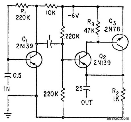
Provides at leaet 200 kc deviation when applied to base of oscillator transistor, before severe distortion sets in. feedback keeps output impedance low.-D. Enemark, Transistors Improve Telemeter Transmitter, Electronics, 32:11, p 136-137. (View)
View full Circuit Diagram | Comments | Reading(1665)
| Pages:12/32 1234567891011121314151617181920Under 20 |
Circuit Categories
power supply circuit
Amplifier Circuit
Basic Circuit
LED and Light Circuit
Sensor Circuit
Signal Processing
Electrical Equipment Circuit
Control Circuit
Remote Control Circuit
A/D-D/A Converter Circuit
Audio Circuit
Measuring and Test Circuit
Communication Circuit
Computer-Related Circuit
555 Circuit
Automotive Circuit
Repairing Circuit