
Communication Circuit
Index 15
Sensitive photoelectric receiver circuit diagram
Published:2011/8/3 2:40:00 Author:Rebekka | Keyword: Sensitive photoelectric receiver
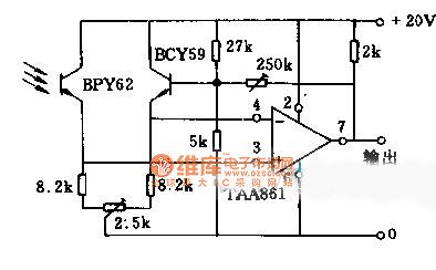
The circuit phototransistor BPY62 isparallel with temperature compensation transistors BCY59. It constitutes a differential amplifier. Two tubes require the same type of product which are matching pairs. The sensitivity can be adjusted by 250KΩ potentiometer. The adjustment margin is 1:5 times. When the average output voltage is 10V, its corresponding light intensity is about 200lx. The adjustment of2.5KΩ potentiometer can calibrate the balance voltage between symmetry and DC. (View)
View full Circuit Diagram | Comments | Reading(1559)
QRP_CW_TRANSCEIVER
Published:2009/7/8 22:54:00 Author:May
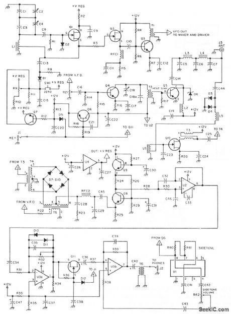
This is a 3-W, single-circuit board, VFO-controlled CW transceiver for 40 or 30 me'ers, featuring a direct-conversion receiver with audio filtering, Receiver Incremental Tuning (RIT). and speaker level audio volume. The transmit frequency is generated by Q1 and its associated component in the VFO The buffer, Q2, isolates the oscillator from the other circuitry to help the VFO stable.Q3 builds up the signal to a more usable level. The driver, Q4, amplifies the signal. The final, Q5, amplifies it to the 3-W level.Key the transmitter by turning the power to the driver on and off using Q6 as a switching transistors Selec.the frequency by varying the,tuning capadtor, C2. The VFO frequency feeds into the diode-ring mixer, and is mixed with the incoming 7-or 10-MH, signal. The difference or produce,is the audio frequency. The post-mixer circuitry amplifies the audio sianal to speaker leve Q8 preamplifies the signal a little, U2 is an audio filter that attenuates the audio signals above about 700 Hz, and U3 amplifies the signal from the audio filter to listening level. (View)
View full Circuit Diagram | Comments | Reading(2826)
LINE_CURRENT_DETECTOR
Published:2009/7/8 22:47:00 Author:May
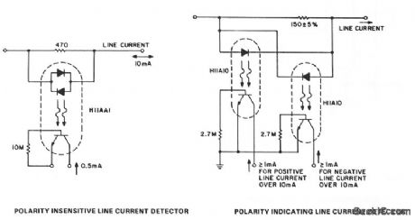
Detection of line-current flow and indicating the flow to an electrically remote point is required in line status monitoring at a variety of points in the telephone system and auxiliary systems. The line should be minimally unbalanced or loaded by the monitor circuit, and relatively high levels of 60-Hz induced voltages must be ignored. The H11AA1 allows line currents of either polarity to be sensed without discrimination and will ignore noise up to approximately 2.5 mA. In applications where greater noise immunity or polarity-sensitive line-current detection is required, the H11A10 threshold coupler can be used. This phototransistor coupler is specified to provide a minimum 10% current transfer ratio at a defined input current, while leaking less than 50 μA at half that input current over the full -55℃ to + 100℃ temperature range.The input current range, at which the coupler is on, is programmable by a single resistor from 5 to 10 mA. (View)
View full Circuit Diagram | Comments | Reading(1322)
A_ONE_TRANSISTOR_FM_TRANSMITTER
Published:2009/7/8 22:40:00 Author:May
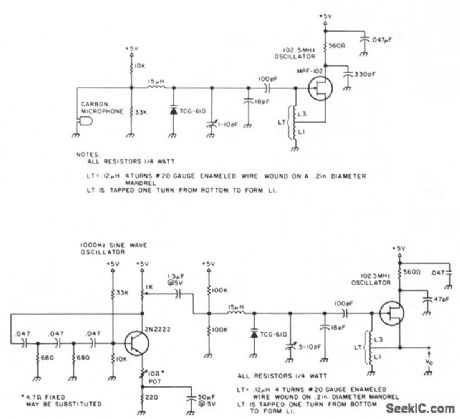
The 2N2222 circuitry is a three-element, phase-shift oscillator circuit, designed to yield a 1,000-Hz sine wave. The 1,000-Hz sine wave is then applied to the TCG-610 varactor diode, 6 pF at 4 V, which changes the tank capacitance, thus varying the rf oscillator frequency at a 1,000-Hz rate. The 1,000-Ω potentiometer in the collector circuit can be adjusted to enable the desired frequency modulation level.The Hartley rf oscillator, designed around a readily available MPF-102 JFET, has an output that should be relatively stable if it is enclosed in a metal box, thus minimizing changes in tank capacitance. The completed transmitter has a range of 30 feet when not enclosed-without an antenna. (View)
View full Circuit Diagram | Comments | Reading(3127)
902_MHz_CW_TRANSMITTER
Published:2009/7/8 22:36:00 Author:May
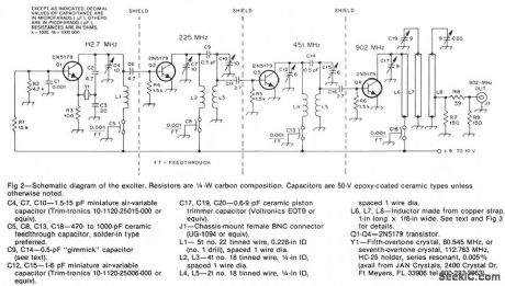
The oscillator, Q1, is a standard overtone circuit. A fifth-overtone crystal, 80.545 MHz, is operated on the seventh overtone, 112.763 MHz. C6 couples the output of the oscillator to Q2, which operates as a doubler to 225.5 MHz. A double-tuned circuit using C7, L2, L3, C10 is used in the collector of Q2 to reduce the level of the 112-MHz oscillator signal. The output of Q2 is capacitively coupled at C11 to the base of Q3. The double-tuned circuit in the collector of Q3 with C12, L4, L5, C15, is tuned to 451 MHz. A small capacitance, 2.7 pF, couples the 451-MHz signal to the base of another 2N5179, Q4, which doubles the signal to 902 MHz. The output of the 902-MHz doubler has a triple-tuned circuit using C17, L6, C19, L7, C20, L8 in its collector.
(View)
View full Circuit Diagram | Comments | Reading(1492)
40_W_CM_TRANSCEIVER
Published:2009/7/8 22:24:00 Author:May
The unit consists of a direct conversion receiver and 1-W transmitter. The direct conversion receiver VFO is tuned just off frequency from the incoming signal. This difference in frequency produces a clean, strong, and solid audio tone signal. Detect the resonant frequency of the transmitter VFO by using the GDO as a field-strength meter.Because of the large capacitance in the Colpitts VFO, the tuning coil will have fewer turns than the mixer coil. Use the capacitance shown for the VFO gate to ground and to the coil. It will effect the fre-quency and output. You'll need 1.4-V rms on pin 2 of the mixer to get a good signal from the VFO. The 1000-Ω resistor and 0.01-μF capacitors act as an rf filter from the mixer output. (View)
View full Circuit Diagram | Comments | Reading(1138)
LM1812 (industrial control, communication and alarm equipment) ultrasonic remote control transmitting or receiving circuit
Published:2011/8/2 3:17:00 Author:TaoXi | Keyword: industrial control, communication, alarm equipment, ultrasonic, remote control, transmitting, receiving circuit
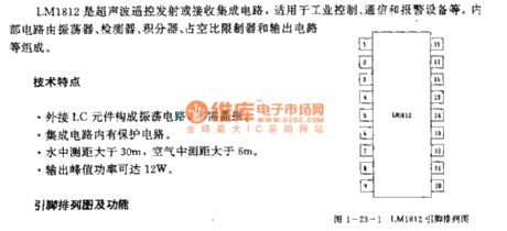
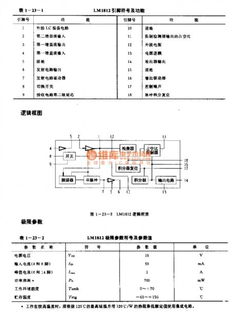
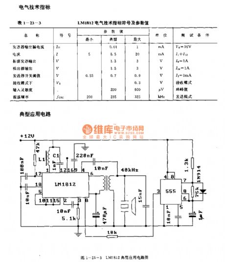
The LM1812 is designed as the ultrasonic remote control transmitting or receiving circuit that can be used in the industrial control, communication and alarm equipment applications. The internal circuit is composed of the oscillator, the detector, the integrator, the duty ratio limiter and the output circuit.
Features
The external LC components form the oscillating circuit, it does not need the crystal oscillator.The IC has the protection circuit.The measuring distance in the water is more than 30m, the measuring distance in the air is more than 6m.The peak value of the output power can be 12W.
(View)
View full Circuit Diagram | Comments | Reading(2014)
BEACON_TRANSMITTER
Published:2009/7/8 22:10:00 Author:May
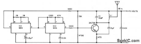
This transmitter can be used for transmitter hunts, for remote key finding, or for radio telemetry in model rockets. It can be tuned to the two meter band or other VHF bands by charging C1 and L1. L1 is four turns of #20 enameled wire airwound, 0.25 inch in diameter (use a drill bit), 0.2 inch long, centertapped. The antenna can be 18 inches of any type of wire. IC2 functions as an audio oscillator that is turned on and off by IC1 about once per second. The range of the transmitter is several hundred yards.
(View)
View full Circuit Diagram | Comments | Reading(1276)
LOW_FREQUENCY_TRANSMITTER
Published:2009/7/8 22:04:00 Author:May
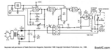
The crystal oscillator, which uses two sections of IC1, a 4001 quad 2-input NOR gate, is a standard and reliable design. The oscillator's 1.85-MHz, square-wave output feeds IC2, a 4017 divide-by-10 counter. The count enable and reset terminals, pins 13 and 15, are normally held high by resistor R3, and the counter is activated by bringing those pins low by closing telegraph key S1-an arrangement that guarantees that the final state of IC2 pin 12 is always high. The high on IC2 pin 12 is inverted by a third section of the 4001, IC1c, to prevent dc current flow through power amplifier Q1 during key-up periods. (View)
View full Circuit Diagram | Comments | Reading(1890)
TA7333F (electronic toy) wireless remote control launch circuit
Published:2011/8/2 4:09:00 Author:TaoXi | Keyword: electronic toy, wireless, remote control, launch circuit
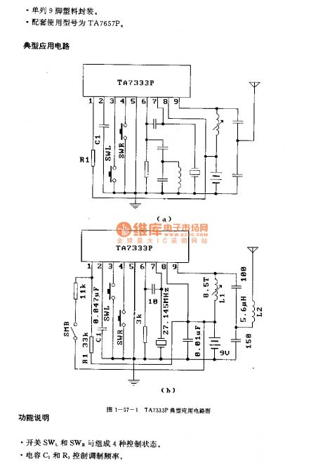
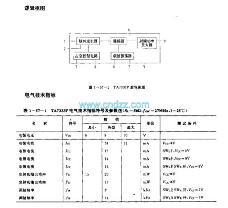
The TA7333P is designed as the wireless remote control launch circuit that can be used in the electronic toy application. The internal circuit is composed of the pulse generator, the mixer, RF power amplifier, duty ratio control circuit and the carrier frequency oscillator.
Features
It has little external components.The operating voltage range is wide (Vcc=6-10V).It is in the single-row 9-pin plastic package.The matching model is TA7657P.
Function description:
The switches SWL and SWR form the four kinds of control states.The capacitors C1 and R1 control the modulation frequency.
(View)
View full Circuit Diagram | Comments | Reading(1747)
1_OF_8_OHANNEL_TRANSMISSION_SYSTEM
Published:2009/7/8 21:59:00 Author:May
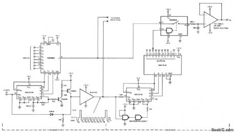
This circuit shows a typical multiplex system intended to carry one of 8 inputs into a remote location.A 5-V pulse train is sent down a separate channel to perform timing and synchronizing functions. A 15-V reset pulse is superimposed on the 5-V clock, which is detected by the MM74C00 in the receiver. Using this system, many remote points can be monitored, one at a time, at any of several locations. (View)
View full Circuit Diagram | Comments | Reading(1127)
LOW_COST_HALF_DUPLEX_INFORMATION_TRANSMISSION_LINK
Published:2009/7/8 21:37:00 Author:May
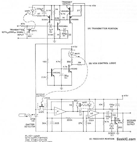
In a half-duplex system, information can flow in both directions, but only one direction at any given time. The conventional method of building a half-duplex link requires a separate emitter and detector, connected with directional couplers, at each end of the fiber. The GFOEIA series of infrared emitting diodes are highly efficient, long-lived emitters, which are also sensitive to the 940 nm infrared they produce. Biased as a photodiode, they exhibit a sensitivity of about 30 nA per μW irradiation at 940 nm. In a suitable bias and switching logic network, they form the basis for a half-duplex information link. A half-duplex link, illustrating the emitter-detector operation of the GFOE1A1, is shown.This schematic represents a full, general purpose system, including: approximately 50-dB compliance range with 1-V rms output, passive receive, voice-activated switching logic, 100 Hz to 50 kHz frequency response, and inexpensive components and hardware. The system is simple, inexpensive, and can be upgraded to provide more capability through use of higher gain bandwidth amplifier stages. Conversely, performance and cost can be lowered simply by removing undesired features. (View)
View full Circuit Diagram | Comments | Reading(1191)
1_W_CW_TRANSMITTER
Published:2009/7/8 21:31:00 Author:May
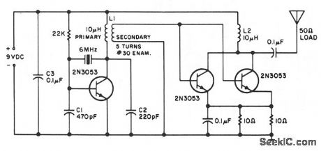
This is a little transmitter that could be put into a plastic Easter egg. It delivers approximately 1 W of measured rf output into a 50-Ω dummy load, and creates no heating problems with the circuit. The crystal is a series fundamental type, and the power source provides 9 V with a 2-A supply. The transmitter can operate at another frequency, but C1 and C2 might have to be changed for the circuit to work properly. The secondary of L1 is wound over the center of a 10- μH coil, with five turns of #30 enameled wire. (View)
View full Circuit Diagram | Comments | Reading(1851)
FM_VOICE_TRANSMITTER
Published:2009/7/8 21:27:00 Author:May

This is a sensitive, mini-powered FM transmitter consisting of an rf oscillator section interfaced with a high-sensitivity wide passband audio amplifier and capacitance microphone with built-in FET that modulates the base of the rf oscillator transistor. The setting of C8 determines the desired operating frequency-in the standard FM broadcast band, tuned to favor the high end up to 110 MHz. Capacitor C7 supplies the necessary feedback voltage developed across R11 in the emitter circuit of Q2, sustaining an oscillating condition. Resistors R9 and R10 provide the necessary bias of the base-emitter junction for proper operation, and capacitor C10 bypasses any rf to ground fed through to the base circuit. C9 provides an rf return path for the tank circuit of L1 and C8, while blocking the dc supply voltage fed to the collector of Q2. The speech voltage developed across R1 by M1 is capacitively coupled by C4 to the base of Q1. A signal voltage developed across R4 is capacity-coupled through C6 to the base of Q2 through R8. R7 and R8, along with C1 and C2, decouple the oscillator and audio circuits. (View)
View full Circuit Diagram | Comments | Reading(1295)
TEMPERATURE_TO_FREQUENCY_CONVERT_ER
Published:2009/7/8 5:29:00 Author:May
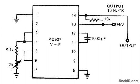
Temperature sensor on chip of AD537 voltage-to-frequency converter IC minimizes number of external parts needed. Output frequency changes 10 Hz for each degree (kelvin or Celsius) change in temperature.-J. Williams, De-signer's Guide to: Temperature Measurement, EDNMagazine, May 20, 1977, p 71-77. (View)
View full Circuit Diagram | Comments | Reading(1170)
25_W_AIRCRAFR_AM_TRANSMΠTER
Published:2009/7/8 5:15:00 Author:May
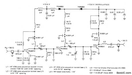
Oper-atesfrom 13.6-V supply,covers frequency rangeof 118-136 MHz without tuning,and has 50-ohm input and output terminations. Only three transistor stages are required. Diodes limit downward modulation to Q2. Upward modu-lation is 95%. Supply drain is 345 mA.- A 13-W Broadband AM Aircraft Transmitter, Moto-rola, Phoenix, AZ, 1974, AN-507, p 5. (View)
View full Circuit Diagram | Comments | Reading(1333)
500_mW_ON_180_kHz
Published:2009/7/8 5:11:00 Author:May
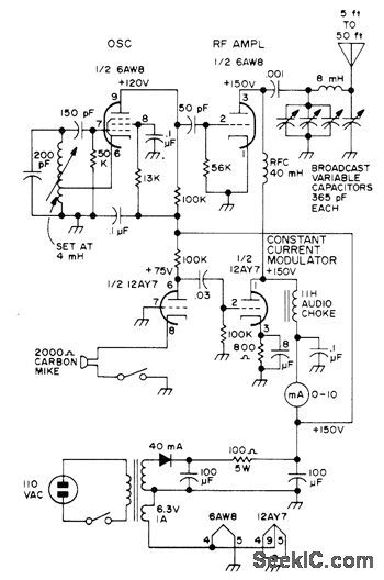
Meets FCC requirement for amateur radio operation in 160-190 kHz band with 1-W maximum plate input power and antenna up to 50 feet long including lead-in.Working range is about 1 mile. Uses electron-coupled oscillator to minimize frequency shift during modulation. RF amplifier is self-biased.40-mH choke in amplifier plate circuit is nearly self-resonant to 180 kHz.-C. Landahl, QRP on 180 kHz, 73 Magazine, May 1973, p 93-95. (View)
View full Circuit Diagram | Comments | Reading(1435)
TEMPERATURE_TO_FR_EOUENCY_CONVERT_ER
Published:2009/7/8 5:08:00 Author:May
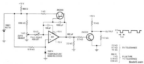
Frequency of relaxation oscillator varies linearly with temperature-dependent voltage across 1N914 diode sensor, with range of 0-1000 Hz for 0-100°C. Frequency meter at output shows temperature directly with accuracy of±0.3°C. Opamp is used as integrator, With 1N821 temperature-compensated diode providing voltage reference that determines firingpoint of UJT Circuit functions as voltage-to-frequency converter, Calibrate at 100°C and 0°C,repeating until adjustments cease to interact,Output frequency is then to times Celsius temperature.-J. Williams and T. Durgavich, Direct-Reading Converter Yields Temperature, Ele-tronics, April3, 1975, p 101 and 103; reprinted in Circuits for Electronics Engineers, Elec-tronics, 1977, p 366.
(View)
View full Circuit Diagram | Comments | Reading(1102)
80_M_AMATEUR_RADIO_TRANSMITTER
Published:2009/7/8 4:55:00 Author:May
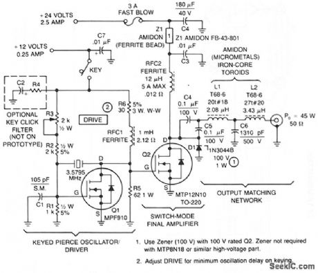
This transmitter consists of a keyed crystal oscillatoridriver and a high efficiency final, each with a TMOS Power FET as the active element. The total parts cost less than $20, and no special construction skills or circuit boards are required.The Pierce oscillator is unique because the high CRSS of the final amplifier power FET, 700 - 1200 pF, is used as part of the capacitive feedback network. In fact, the oscillator will not work without Q2 installed. The MPF910 is a good choice for this circuit because the transistor is capable of driving the final amplifier in a switching mode, while still retaining enough gain for oscillation. To minimize cost, a readily-available color burst TV crystal is used as the frequency-determining element for Q1.An unusual 84% output efficiency is possible with this transmitter. Such high efficiency is achieved because of the TMOS power FET's characteristics, along with modification of the usual algorithm for determining output matching. (View)
View full Circuit Diagram | Comments | Reading(1865)
TRACER_RECEIVER
Published:2009/7/8 4:04:00 Author:May
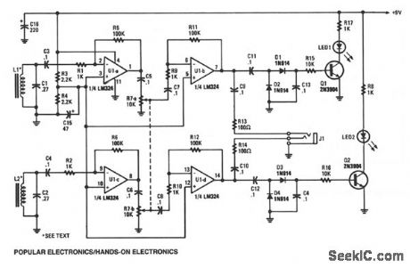
The tracer receiver is a stereo audio amplifier/detector circuit operating near 1 kHz. Inductors L1 and L2-hand-wound coils, consisting of 200 turns of #26 wire on 2-inch ferrite cores- are tuned to the operating frequency of the amplifier/detector. The received signal strength of each individual receiver is indicated by an LED. The audio output of the receiver is fed to a stereo headphone. That dual-receiver scheme helps in locating and tracking the hidden wire or cable by giving a directional output that indicates the cable's path.
The 1-kHz signal is picked up by L1 and coupled to the input of op amp U1a, which provides a gain of about 100 dB. The output of op amp U1a is fed through volume-control potentiometer R7 to the input of U1b, which magnifies the already amplified signal 100 times more. That puts the maximum gain of the receiver at about 10,000 dB. The output of U1b follows two paths: in the first path, the signal is couple through C9 and R13 to J1, and is used to drive one half of a stereo headphone.
In the other path, the signal is fed through a voltage doubling/detector circuit-consisting of Dl, D2, C11, and C13-that converts the amplified 1-kHz signal to the dc voltage that's used to drive Q1. When Q1 is turned on, LED1 lights, indicating a received signal. (View)
View full Circuit Diagram | Comments | Reading(3486)
| Pages:15/32 1234567891011121314151617181920Under 20 |
Circuit Categories
power supply circuit
Amplifier Circuit
Basic Circuit
LED and Light Circuit
Sensor Circuit
Signal Processing
Electrical Equipment Circuit
Control Circuit
Remote Control Circuit
A/D-D/A Converter Circuit
Audio Circuit
Measuring and Test Circuit
Communication Circuit
Computer-Related Circuit
555 Circuit
Automotive Circuit
Repairing Circuit