
Communication Circuit
Index 18
CARRIER_SYSTEM_TRANXMITTER
Published:2009/7/3 5:03:00 Author:May
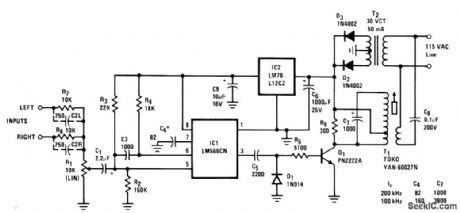
Used to convert audio program material into FM format for coupling to standard power Iines. Modulated FM signal can be detected at any other outlet on same side of distribution transformer, for demodulation and drive of loudspeaker.Input permits combining stereo signals for mono transmission to single remote Ioudspeaker. Uses National LM566CN VCO. Frequency response is 20-20,000 Hz, and total harmonic distortion is under O.5% With 120/240 V power lines, system operates equally well with receiver on either side of line. Transmitter input can be taken from monitor or tape output jack of audio system.-J. Sherwin, N. Sevastopoulos, and T. Regan, FM Remote Speaker System, National Semiconductor, Santa Clara, CA, 1975, AN-146. (View)
View full Circuit Diagram | Comments | Reading(1989)
TTL_TO_CMOS_TRANSLATOR
Published:2009/7/2 5:03:00 Author:May
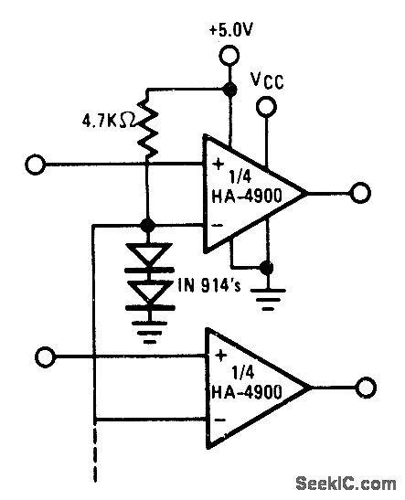
Two sections of Harris HA-4900/4905 precision quad comparator provide intelface between TTL drive and CMOS output circuits. Supply is±15 V.- Linear & Data Acquisition Products, Hatris Semicon-ductor, Melboume, FL, Vol. 1, 1977, p 2-95. (View)
View full Circuit Diagram | Comments | Reading(917)
20_KILOBIT_FIBER_OPTIC_RECEIVER
Published:2009/7/2 3:33:00 Author:May
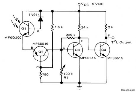
Phototransistor driving three-transistor amplifier provides TTL output for data rates up to 20 kilobits.- Basic Experimental Fiber Optic Systems, Motorola, Phoenix, AZ, 1978. (View)
View full Circuit Diagram | Comments | Reading(1893)
50_kHz_FM_OPTICAL_TRANSMIlTER
Published:2009/7/2 3:05:00 Author:May
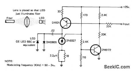
Uses pulse-rate modulation system with center frequency of 50 kHz. Audio fed into transmitter varies pulse rate, for driving LED coupled to optical fiber. Phototransistor at other end of fiber receives and demodulates light signal for reconstruction of audio.-I. Math, Math's Notes, Ca July 1977, p 67-68 and 90. (View)
View full Circuit Diagram | Comments | Reading(1639)
1_10_100_KILOBIT_FIBER_OPTIC_RECEIVER
Published:2009/7/2 3:02:00 Author:May
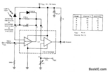
Choice of input device determines operating speed of receiver. MC3405 contains two opamps and two comparators, permitting use as two-channel receiver. Table gives pin connections foi each channeL- Basic Experimental Fiber Optic Systems, Motorola, Phoenix, AZ, 1978. (View)
View full Circuit Diagram | Comments | Reading(1623)
50_kHz_FM_OPTICAL_RECEIVER
Published:2009/7/2 3:00:00 Author:May
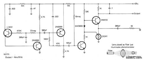
Designed for pulse-rate modulation system in which transmitter varies pulse rate of modulated light beam in optical-fiber cable above and below center frequency of 50 kHz. L14G2 GE photo transistor converts modulated optical light to RF signal for demodulation and reconstruction of original audio. Based on circuit in General Electric Opto-Electronics Manual. -I. Math, Math's Notes, CQ, July 1977, p 67-68 and 90. (View)
View full Circuit Diagram | Comments | Reading(1845)
FIBER_OPTIC_RECEIVER
Published:2009/7/2 2:55:00 Author:May
Uses MFOD100 PIN photodiode as optical detector for handling megabit data rates. Minimum photocurrent required to drive LF357 opamp U1 is 250 nA, Voltage comparator U2 inverts output of U1 and provides standard TTL output. For CMOS output, quad two-input NAND gate U3 is wired into circuit, with jumper J1 connected from U3 output to output terminal of receiver. Adjust R1 to give accurate reproduction of 1-MHz square wave with 50% duty cycle at receiver output.- Basic Experimental Fiber Optic Systems, Motorola, Phoenix, AZ, 1978. (View)
View full Circuit Diagram | Comments | Reading(0)
FIBER_OPTIC_TRANSMTTER
Published:2009/7/2 2:13:00 Author:May
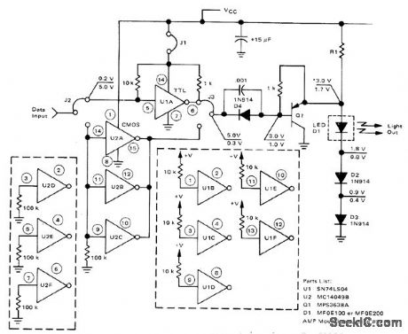
Will handle NRZ data rates to 10 megabits or square waves to 5MHz。 Input is rrL- or CMOS-compatible depending on circuit selected.Transmitter drawsonly 150 mA from 5-V supply for TTL or from 5-15 V supply for CMOS Choose RI to glve LED drive current for proper operation of system For TTL operation,jumpers J1,J2,and J3 are connected as shown. For CMOS operation, remove J1 and transfer J2 and J3 to altemate positions for connecting to U2. Choice of LED depends on system length and desired data rate.Power supply can be HP6218A or equivalent. DC voltages shown are for TTL interface, with uppervaluefor LED on at 50 mA and lowervalue for LED off.- Basic Experimental Fiber Optic Systems, Motorola, Phoenix, AZ, 1978. (View)
View full Circuit Diagram | Comments | Reading(1432)
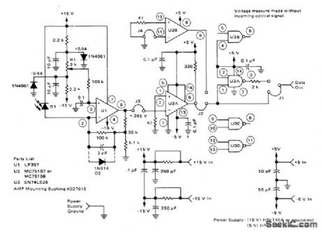
10_MHz_FIBEROPTIC_RECEIVER
Published:2009/7/1 23:36:00 Author:May
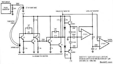
The receiver will accurately condition a wide range of light inputs at up to 10 MHz data rates.The optical signal is detected by the PIN photodiode and amplified by a broadband fed-back stage, Q1-Q3. A second, similar, stage gives further amplification.The output of this stage (Q5's collector) biases a 2-way peak detector (Q6-Q7). The maximum peak is stored in Q6's emitter capacitor while the minimum excursion is retained in Q7's emitter capacitor. The dc value of Q5's output signal's mid-point appears at the junction of the 0.005μF capacitor and the 22 M ohm unit. This point will always sit midway between the signal's excursions, regardless of absolute amplitude. This signal-adaptive voltage is buffered by the low bias LT1012 to set the trigger voltage at the LT1016's positive input. The LT1016's negative input is biased directly from Q5's collector. (View)
View full Circuit Diagram | Comments | Reading(1682)
PULSE_COINCIDENCE_DETECTOR
Published:2009/7/1 21:18:00 Author:May
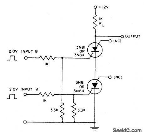
Unless inputs A and B (2- to 3-V amplitude) occur simultaneously no voltage exists across RL. Less than 1 microsecond overlap is sufficient to trigger the scs. Coincidence of negative inputs is detected with gates GA instead of GC by using the scs in a complementary SCR configuration. (View)
View full Circuit Diagram | Comments | Reading(0)
4_CHANNEL_COMMUTATOR
Published:2009/7/1 21:16:00 Author:May
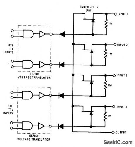
This 4-channel commutator used the 2N4091 to achieve low channel on resistance (<30 ohm) and low off current leakage. The DS7800 voltage translator is a monolithic device that provides from 10 V to -20 V gate drive to the JFETs while at the same time providing DTL/TTL logic compatibility. (View)
View full Circuit Diagram | Comments | Reading(1076)
ASTABLE_USING_CMOS_TRANSISTOR_PAIR
Published:2009/7/1 20:12:00 Author:May
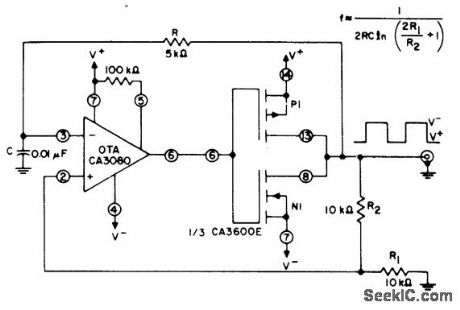
One transistor pair from CA3600E array is used with CA3080 operational transconductance amplifier to give precise timing and threshold for square waves,Quiescent power consumption is typically 6 mW with values shown.-''Linear Integrated Circuits and MOS/FET’s.''RCA Solid State Division, Somerville、NJ、1977, p 279. (View)
View full Circuit Diagram | Comments | Reading(2330)
FM_DEMODULATOR
Published:2009/7/1 5:14:00 Author:May
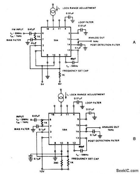
The NE564 is used as an FM demodulator. The connections for operation at 5 V and 12 V are shown in Figures 21-4A and 21-4B. The input signal is ac coupled with the output signal being extracted at Pin 14. Loop filtering is provided by the capacitors at Pins 4 and 5 with additional filtering being provided by the capacitor at Pin 14. Since the conversion gain of the VCO is not very high, to obtain sufftcient demodulated output signal the frequency deviation in the input signal should be 1% or higher. (View)
View full Circuit Diagram | Comments | Reading(0)
TRANSISTORS_FOR_BC_221
Published:2009/7/1 5:07:00 Author:May
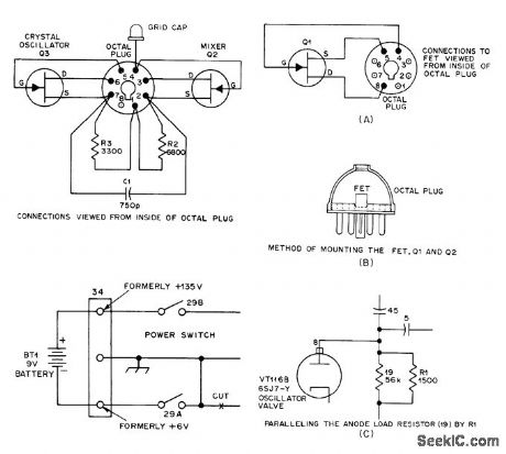
TRANSISTORS FOR BC-221-Old BC-221 frequency meter can be modernized by replacing its three now-scarce tubes with four 2N3819 Nchannel JFETs and changing supply to single 9 V battery. VT167 (6K8) mixer-oscillator is replaced by two JFETs with R2, R3, and 01 mounted inside octal plug. Resistance values may need some adjustment. Cut and insulate original leads to pins 2, 4, and 7, and connect top-cap clip of mixer tube to pin 4. VT116-B (6SJ7-Y) tube used for VFO is replaced by single 2N3819 connected as for Q1.Place 4K across 15K Add RI in parallel with plate load resistor; value depends on par-ticular FET used, and can range from 1 to 6800 ohms (1500 is typical). VT116 (6SJ7) beat-fre-quency amplifier is replaced by 2N3819 mounted same as for al. Place 4K across 15K load resistor of VT116-B and replace 300-ohm cathode resistor with one giving 1-mA source current (typically 1K to 3.3K). Total current drain is about 3 mA. Try 3-10 pF capacitor between gate and drain of 03 if circuit does not oscil-Iate.-R. S. N. Rau, Solid-State BC-221 Fre-quency Meter, 0ST, Feb. 1977, p 35-36. (View)
View full Circuit Diagram | Comments | Reading(3012)
INFRARED_RECEIVER
Published:2009/7/1 0:56:00 Author:May
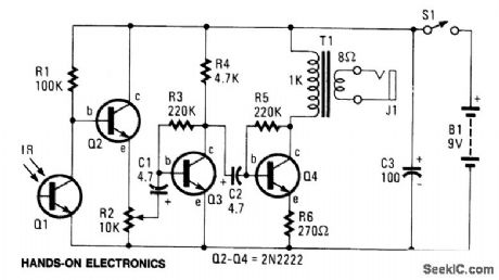
The circuit consists of Q1-a phototransistor that responds to an intensity of amplitude-modulated IR light source-and a three-stage, high-gain audio amplifier.Transformer T1 is used to match the output impedance of the receiver to today's popular low-impedance (low-Z) headphones; but if a set of 1000-2000 ohm, magnetic (not crystal), high-impedance (high-Z) phones are to be used, remove T1 and connect the high-Z phones in place of T1's primary winding-the 1000-ohm winding. (View)
View full Circuit Diagram | Comments | Reading(2242)
INFRARED_TRANSMITTER_1
Published:2009/7/1 0:54:00 Author:May
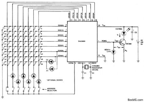
The transmitter keyboard is arranged as a scanned matrix. The matrix consists of 7 driver outputs and 7 sense inputs. The driver outputs DRVON to DRV6N are open-drain n-channel transistors and they are conductive in the stand-by mode. The 7 sense inputs (SENON to SEN6N) enable the generation of 56 command codes. With 2 external diodes all 64 commands are addressable. The sense inputs have p-channel pull-up transistors, so that they are HIGH until they are pulled LOW by connecting them to an output via a key depression to initiate a code transmission. (View)
View full Circuit Diagram | Comments | Reading(0)
INFRARED_TRANSMITTER
Published:2009/7/1 0:53:00 Author:May
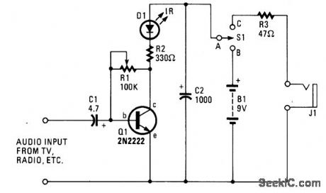
The ultra-simple one-transistor, IR transmitter shown is designed to transmit the sound from any 8 or 16 ohm audio source, such as a TV, radio, or tape recorder on an infrared beam of light. (View)
View full Circuit Diagram | Comments | Reading(2265)
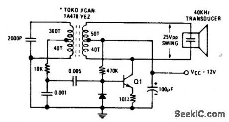
40_kHz_ULTRASONIC_TRANSMITTER_1
Published:2009/6/30 21:06:00 Author:May
View full Circuit Diagram | Comments | Reading(1117)
40_kHz_ULTRASONIC_TRANSMITTER
Published:2009/6/30 3:23:00 Author:May

View full Circuit Diagram | Comments | Reading(1124)
SIMPLE_FM_TRANSMITTER
Published:2009/6/30 3:10:00 Author:May
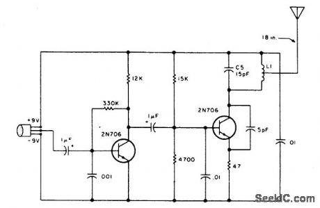
This transmitter can be tuned to the FM broadcast band, 2 meters, or other VHF bands by changing C5 and L1. The values given for C5 and L1 will place the frequency somewhere in the FM broadcast band. L1 is 4 turns of #20 enameled wire airwound, Y4 inch in diameter, 5mm long and center-tapped. The microphone is an electret type and the antenna is 18 inches of any type of wire. Keep all leads as short as possible to minimize stray capacitance. The range of the transmitter is several hundred yards. (View)
View full Circuit Diagram | Comments | Reading(0)
| Pages:18/32 1234567891011121314151617181920Under 20 |
Circuit Categories
power supply circuit
Amplifier Circuit
Basic Circuit
LED and Light Circuit
Sensor Circuit
Signal Processing
Electrical Equipment Circuit
Control Circuit
Remote Control Circuit
A/D-D/A Converter Circuit
Audio Circuit
Measuring and Test Circuit
Communication Circuit
Computer-Related Circuit
555 Circuit
Automotive Circuit
Repairing Circuit