
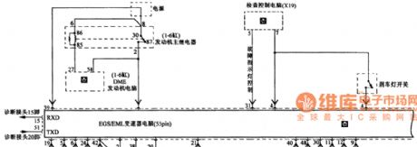
Communication Circuit
Index 7
BMW7 Series EGS / EML 55pin Transmission Circuit (the 2nd)
Published:2011/7/17 21:43:00 Author:Felicity | Keyword: BMW7 Series, EGS / EML 55pin, Transmission Circuit, (the 2nd)
View full Circuit Diagram | Comments | Reading(1194)
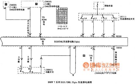
BMW7 Series EGS / EML 55pin Transmission Circuit (the 1st)
Published:2011/7/17 21:42:00 Author:Felicity | Keyword: BMW7 Series, EGS / EML 55pin, Transmission Circuit, (the 1st)
View full Circuit Diagram | Comments | Reading(1070)
BMW7 Series EGS / EML 35pin Transmission Circuit (the 2nd)
Published:2011/7/17 21:50:00 Author:Felicity | Keyword: BMW7 Series, EGS / EML 35pin, Transmission Circuit, (the 2nd)
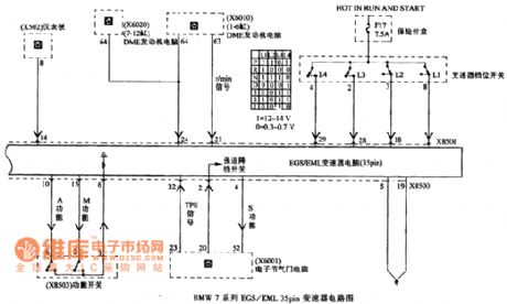
View full Circuit Diagram | Comments | Reading(1121)
VIDEO_MONITOR_TERMINATOR
Published:2009/7/14 21:43:00 Author:May
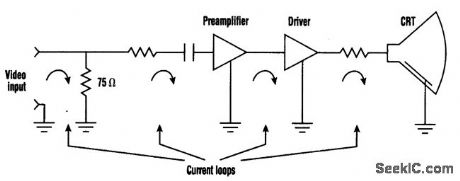
The best method of terminating video output signals is to route the video cable directly to the video-amplifier input connector without connecting its signal or shield wires to other parts of the monitor. (View)
View full Circuit Diagram | Comments | Reading(1124)
SINGLE_IC_TOUCH_TONE_ENCODER
Published:2009/7/14 21:58:00 Author:Jessie
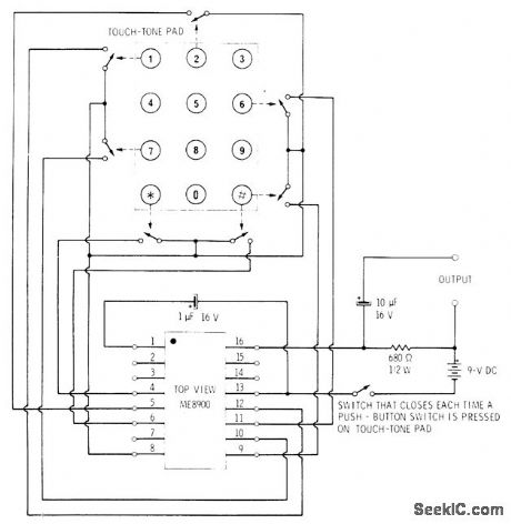
Uses ME8900 tone generator made by Microsystems International, Ottawa, Canada, to generate pairs of audio frequencies for telephone signaling. Standard Touch-Tone pad provides column and row switch closures for pins 4, 5, 6, and 8 going to low-frequency parallel-T oscillators of IC and for pins 9, 10, 11, and 12 of high-frequency oscillator-C. D. Rakes, Integrated Circuit Projects, Howard W. Sams, Indianapolis, IN, 1975, p 100-101. (View)
View full Circuit Diagram | Comments | Reading(1837)
SIMPLE_VIDEO_RECEIVER
Published:2009/7/14 21:28:00 Author:May
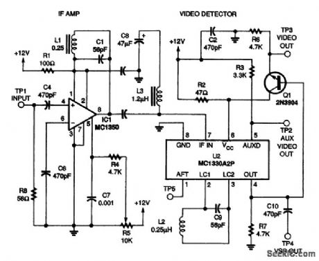
The IF input from the tuner is fed into an MC1350 amplifier (IC1) through capacitor C4. The 56Ω input resistor R8 approximates the impedance of the tuner's 50-Ω output. The IF amplifier is tuned by variable inductor L1 and capacitor C1, and its gain is controlled by potentiometer R5. The output of the IF amplifier is coupled into an MCl330 low-level video detector (IC2) through C5. The optional LC trap circuit, consisting of C8 and L3, can be adjusted to eliminate a specific signal, but the circuit will work well without the trap. The MC1330 is also tuned with a tank circuit, consisting of L2 and C9. The video outputs are biased with resistor networks. The noninverted video is fed into the base of a 2N3904 NPN transistor Q1 configured as a unity-gain, common-collector, buffer amplifier for impedance matching. The primary video output is taken from the top of Q1's emitter resistor R6, and the auxiliary video output is taken from pin 5 of IC2. The VSB output is an ac-coupled version of the primary output, and it can be used for any sound output you wish to use in the future, The switching carrier output can be used for automatic fine-tuning (AFT) circuits. (View)
View full Circuit Diagram | Comments | Reading(5075)
567_ULTRASONIC_RECEIVER
Published:2009/7/14 21:24:00 Author:May
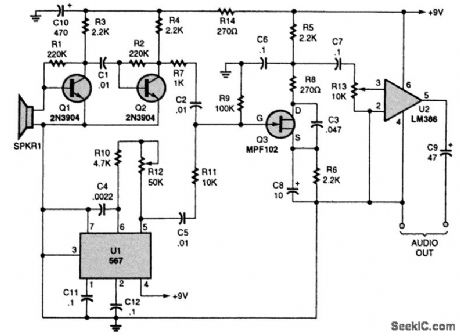
This tunable ultrasonic receiver is ideal for use with the ultrasonic transmitter. It, too, is built around a 567 PLL. (View)
View full Circuit Diagram | Comments | Reading(3195)
CRT_TUNING_INDI_CATOR
Published:2009/7/15 2:08:00 Author:Jessie
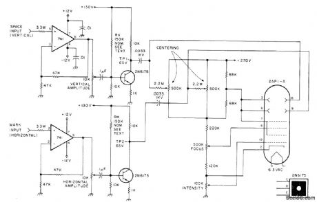
Crossed -ellipse display on CRT aids in tuning receiver to RTTY signal. Display shows at a glance if station is narrow or wide, or if other station is transmitting upside-down signals (mark and space frequencies reversed). Tuned for maximum amplitude of major axis of each ellipse; if transmitting station is wide or narrow, tune for equal amplitudes even though they are not maximized. Try different values of RV until T.P.1 voltage is 65 V, to center signal so it can swing equal amounts on either side Adjust RH similarly-R.R. Parry, RTTY CRT Tuning Indicator, 73 Magazine, Sept 1977, p 118-120. (View)
View full Circuit Diagram | Comments | Reading(1399)
VACUUM_TUBE_TRANSMITTER
Published:2009/7/14 21:11:00 Author:May
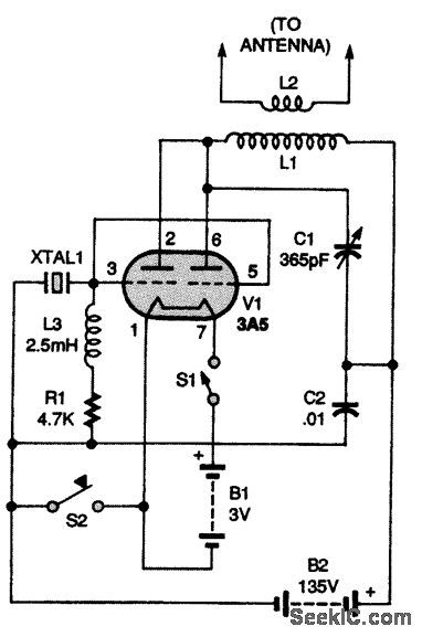
The schematic for the transmitter is shown in the figure. In the circuit, power is supplied by a 3V battery B1 and a 135-V battery B2. The latter battery, B2, can be replaced by a power-supply circuit. Switch S1 is used to turn the circuit on and off. The heart of the circuit is a 3A5 tube, V1. Both sections of V1 are connected in parallel in a conventional Miller oscillator. Resistor R1 sets the bias for the tube; the value of R1 might seem low to some because it is only 4700Ω, but keep in mind that V1 is a transmitting triode operating at class C. A 2.5-mH RF choke coil (L3) is needed to keep the radio frequency where it belongs. Capacitor C1 and inductor L1 resonate at the frequency of a 40-m (7- to 7.3-MHz) amateur crystal, XTAL1. Inductor L2 couples RF energy to an attached antenna; C2 is a bypass capacitor. Switch S2 is a telegraph-type key switch. That is used to generate the content of any transmissions you make. Transformer T1 provides isolation from the power line. The isolated ac voltage is rectified by diode D1 and filtered by capacitor C1. (View)
View full Circuit Diagram | Comments | Reading(4063)
WIRELESS_CAMCORDER_MICROPHONE
Published:2009/7/14 21:06:00 Author:May
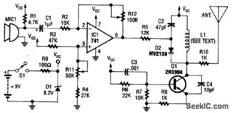
A 741 op amp acts as an audio amplifier and frequency-modulates VHF oscillator Q1 via varactor D2. L1 is 2.5 turns of #18 wire on a 5/16,-inch-diameter form. The turn spacing can be varied to adjust the transmitter frequency. ' (View)
View full Circuit Diagram | Comments | Reading(1851)
AM_TONE_TRANSMITTER
Published:2009/7/14 20:58:00 Author:May
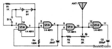
Power for the circuit is supplied by B1, a 9-V battery. Two sections of a 4011 NAND gate, U1-c and U1-d, are used as part of a radio-frequency (RE) oscillator (carrier). The other two sections, U1-a and U1-b, are used in an audio-frequency (AP) oscillator (modulator). Switch S1 enables and disables the modulation to allow the transfer of an intelligent message with the transmitter. When you press S1, the AP oscillator composed of U1-a, U1-b, R4, and C1 starts generating an audio signal.That signal gates the RE oscillator composed of U1-c, U1-d, R2, R3, and C2 on and off. When on, the RE oscillator runs at 1 MHz. The resulting output is sent out ANT1 as an AM signal. (View)
View full Circuit Diagram | Comments | Reading(2730)
BA1404_STEREO_TRANSMITTER
Published:2009/7/14 20:54:00 Author:May

At the heart of the schematic for the FM stereo transmitter is the BA1404 FM stereo transmitter IC. Note that there is no R2 or R5 circuit.
The circuit uses the BA1404 IC (Rohm semiconductor) to implement a complete low-power FM stereo transmitter in the 88- to 92-MHz band. Line-level audio is fed to U1, the BA1404. Xtal1 is a 38-kHz crystal, and the RE oscillator tank C16/L1 (and associated components) determine RE frequency. The circuit should be carefully constructed to minimize frequency drift and microphonics. Q1 is a buffer amplifier to reduce oscillator frequency pulling. A 9-V supply is used to power the circuit. (View)
View full Circuit Diagram | Comments | Reading(6967)
INTERMEDIATE_FREQUENCY_TRANSMITTER
Published:2009/7/14 20:50:00 Author:May
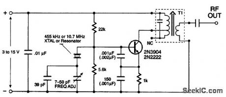
The oscillator transmitter circuit is a variation of the Colpitts configuration. This particular circuit exhibits excellent frequency stability, good isolation between the frequency reference and the output, and isolated low output impedance. If you have the correct crystal on hand, that's fine. If not, a ceramic resonator will also work with the components shown. The tuned circuit T1 is an IF can, salvaged from an old AM and FM receiver; be sure that it has a primary tap. The primary of the 455-KHz, IF can will measure 3 to 5Ω, and the 10.7-MHz IF can will measure less than 1Ω; these measurements will help you to identify the correct inductor. The components in parentheses should be used for the 455-kHz transmitter. (View)
View full Circuit Diagram | Comments | Reading(2819)
LOW_POWER_PLL_STABILIZED_FM_STEREO_TRANSMITTER
Published:2009/7/14 20:47:00 Author:May
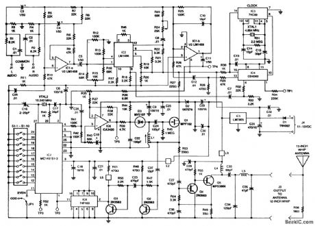
The schematic shows a high-performance FM stereo transmitter, consisting of a stereo generator IC1 (audio matrixing), a balanced modulator IC2, a pilot and subcarrier generator IC3 and IC4, and a PLL synthesizer IC6, IC7, and IC8. Frequencies from 76 to 108 MHz are supported, with 100-kHz resolution. All oscillators are crystal-controlled for stability. The output is 0.5 to 0.7 V into 50 Ω.In the United States, in order to comply with FCC regulations, the transmitter is terminated in a 56Ω resistor, which is nonradiating , and a small whip antenna (up to 12 inches long) is used as a radiating probe. The radiated field must be kept to 250 μV/m at 3 m from the antenna. In open locations, a 4-inch whip should give sufficient range (100 feet typical); for use inside buildings, where some losses are encountered, a 12-inch antenna might be needed. Do not use more than a 12-inch whip. In other nations, where regulations allow, a matched antenna can be used and the output amplifier can be run at 15 V or more, with over 200 mW output possible. Up to 24 V can be used if higher-voltage bypass capacitors are used on the supply line and R27 is changed to 680Ω. IC5 might need heatsinking in this case.
A complete kit of parts, including PC board, is available from North Country Radio, P.O. Box 53, Wykagyl Station, New Rochelle, NY 10804-0053A. (View)
View full Circuit Diagram | Comments | Reading(6032)
STOP_FOR_AUTOSTART
Published:2009/7/15 2:07:00 Author:Jessie
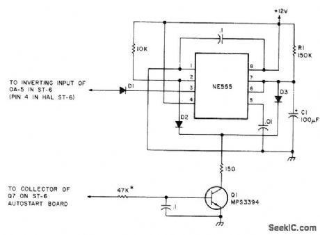
Uses 555 timer IC to make ST-6 autostart turn off motor of teleprinter if copying commercial station that does not drop its carrier when no text is being trans. mitted. Values shown for C1 and R1 give time of 15 s which, added to 25 s of ST-6 delay, gives about 40 s to turn off in presence of steady mark tone (carrier only). Useful when copying weather and press reports.-R. Bourgeois, Stop That Autostart, 73 Magazine, May 1977, p 47. (View)
View full Circuit Diagram | Comments | Reading(1461)
TRANSPARENT_LATCH
Published:2009/7/14 12:03:00 Author:May
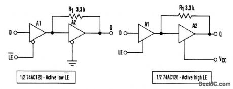
The circuit depicted here, which yields two independent latches per chip, is rather simple and inexpensive to build (see the figure). The second buffer A2 is wired with resistor R1 in the feedback path (ignore A1 for the moment). A2 with feedback resistor R1 is a stable latch. Because of the very low input current requirements of A2, there is hardly any voltage drop across R1. As a result, the input is the same as the output, and that is fed forward through the buffer, mA1ntA1ning a stable level. When buffer A1 is enabled, the input of A2 is driven to the same level as D. Even if A2's output (Q) is at an opposite logic level, which can happen momentarily (for a gate delay) when D is opposite to Q, Al is required to sink or source current through R1. After a gate delay, this signal propagates to Q. Both sides of R1 are now at the same logic level. When the LE signal goes inactive, A1 tristates and the latch will hold the level present at D one setup time prior to LE's going inactive. (View)
View full Circuit Diagram | Comments | Reading(1380)
AFSK_WITH_PLL
Published:2009/7/15 2:05:00 Author:Jessie
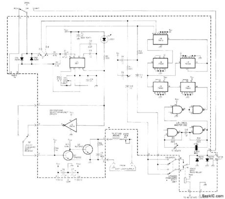
Complete terminal unit and AFSK tone generator for VHF bands synthesizes tones digitally for 170-Hz narrow shift and 850-Hz standard shift found in VHF amateur RTTY bands. Additional feature is PLL circuit that follows drifting signal and copies signals from which mark or space information is missing. Precision AFSK generator consists of 5.95-MHz crystal oscillator U3, divide-by-1 IC U6, and divide-by-2 IC U8, resulting in symmetrical 2975-Hz square wave at pin 12 of U8. Programmable counter U7 divides 59.5 kHz down to 4250 Hz. Other half of U8 divides this by 2, to give symmetrical 2125-Hz squeal wave at pin 9 of U8. Square waves are converted to trapezoids, with tops smoothed by CR3 and CR4, to give 1 V P-P quasi-sine waves at output. Demodulator U1 compares incoming frequencies to its internal current-controlled oscillator and generates digital signals when they are identical. Internal oscillator is locked to incoming signal if within detection bandwidth of about 220 Hz for 2125 Hz with 170-Hz shift. At 2975 Hz, detection bandwidth is about ±135 Hz.-J.Loughmiller, Digiratt-RTTY AFSK Generator and Demodulator, Ham Radio, Sept.1977,p 26-28. (View)
View full Circuit Diagram | Comments | Reading(2835)
LASER_TRANSMITTER_
Published:2009/7/14 11:54:00 Author:May
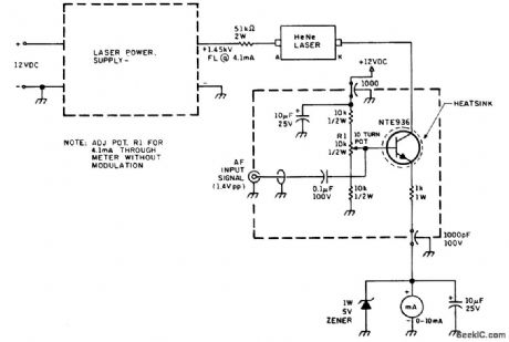
A current modulator is connected to the cathode of the laser. The quiescent current is set at 4.1 mA, and the modulating sigpal is set to vary the current only by ±0.7 mA. A well-protected and by-passed 0- to 10-mA meter is used in the ground leg to set and monitor the laser's quiescent operating current. A 51-kΩ, 2-W ballast resistor close to the anode lead of the laser stabilizes the discharge. The voltage across the sustaining supply should be 1.45 kV dc at full load. Remember that the subcarrier frequency must be no greater than 200 kHz, and that the peak-to-peak signal voltage into the modulator must not exceed 1.4 V p-p. (There are any number of ICs that operate as voltage controlled oscillators to produce the FM subcarrier.) (View)
View full Circuit Diagram | Comments | Reading(1600)
INFRARED_DATA_RECEIVER
Published:2009/7/14 7:43:00 Author:May
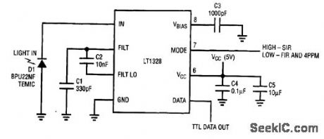
The LT1328 circuit operates over the full 1-cm to 1-m range of the IrDA standard at the stipulated light levels. For IrDA data rates of 115 kb/s and below, a 1.6-μs pulse width is used for a 0 and no pulse for a 1. Light levels are 40 to 500 mW/sr (milliwatts per steradian). The figure shows a scope photo for a transmitter input (top trace) and the LT1328 output (bottom trace). Note that the input to the transmitter is inverted; that is, transmitted light produces a high at the input, which results in a zero at the output of the transmitter. The MODE pin (pin 7) should be high for these data rates. (View)
View full Circuit Diagram | Comments | Reading(1247)
MONO_CORDLESS_HEADPHONE_IR_RECEIVER
Published:2009/7/14 7:37:00 Author:May
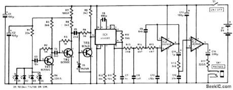
The full receiver circuit diagram appears in the figure. As many as four infrared detector can be used (D1 to D4 ). They are wired in parallel and used in the reverse-biased mode, and dark conditions only very small leakage currents flow. The pulses of infrared from the transmitter result in increased leakage currents, which generate small negative pulses at the cathodes (k) of the diodes. Transistor TR1 is used as a low-noise preamplifier and buffer stage. The majority of the voltage gain is provided by transistors TR2 and TR3, which are also common-emitter stages. These provide a combined voltage gain of over 80dB. The signal from TR3 is connected to one of the phase comparator inputs of IC1 (pin 14 ). This IC provides demodulation and is a CMOS 4046BE p.l.d. Resistor R10 and capacitor C6 are the timing components for the VCO,and they set the center frequency at approximately 100 kHz. Resistor R10 and capacitor C7 form a simple low-pass filter between the phase comparator’s output at pin 2 and the input of the VCO at pin 9. The audio output signal is obtained from the low-pass filter via an integral source-follower stage. The output from IC2 is fed to resistor R16 and capacitor C12, which form a simple low-pass filter that provides the deemphasis. The signal is then fed to the input of IC3, which is a small class-B audio power amplifier. The current consumption of the receiver is about 12 mA. (View)
View full Circuit Diagram | Comments | Reading(1755)
| Pages:7/32 1234567891011121314151617181920Under 20 |
Circuit Categories
power supply circuit
Amplifier Circuit
Basic Circuit
LED and Light Circuit
Sensor Circuit
Signal Processing
Electrical Equipment Circuit
Control Circuit
Remote Control Circuit
A/D-D/A Converter Circuit
Audio Circuit
Measuring and Test Circuit
Communication Circuit
Computer-Related Circuit
555 Circuit
Automotive Circuit
Repairing Circuit