
Communication Circuit
Index 16
20_MHz_PHONE
Published:2009/7/8 2:13:00 Author:May
Colpitts oscillator using HEP 53 provides excellent stability with third-over-tone crystal. Power amplifier stage uses 2N4427 in class C common-emitter stage modulated through collector circuit, to develop about 1.25-W output at 28 MHz. HEP 801 FET microphone amplifier provides high-impedance input for crystal microphone and drives HEP 593 IC to give about 1-W AF output. Article covers con-struction and tune-up.-B. Johnston, Little Bill, 73Magazine, July 1974, p 63-64 and 66-67. (View)
View full Circuit Diagram | Comments | Reading(1597)
INFRARED_TRANSMITTER
Published:2009/7/7 8:28:00 Author:May
View full Circuit Diagram | Comments | Reading(0)
DIGITAL_IR_TRANSMITTER
Published:2009/7/7 8:27:00 Author:May
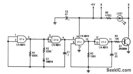
Gates U1a and U1b are configured as a low-frequency oscillator. The output waveform at pin 11 is nonsymmetrical with the positive portion of the signal, making up only 20% of the time period.Diode D1, a 1N914 general-purpose unit, together with C1, R1, and R2, determine the on time for the positive portion of the output waveform. The off, or negative portion of the output waveform, depends mainly on the values of R1 and C1. The operating frequency of that oscillator is about 11 Hz. The second oscillator consists of U1c and U1d, which outputs on almost symmetrical waveform at a frequency of about 400 Hz. The output of first oscillator U1a/U1b is fed to pin 8 of U1c to key second oscillator U1c/U1d on and off at about 11 Hz, with the on time limited to about 20% of the time period (about 15 ms).The output waveform of the second oscillator is fed to the base of Q1, which is used to drive IR diode LED1 in short bursts. Pulsing LED1 helps to save battery power, and also allows each circuit to be given its own special sound footprint.By changing any of the values of R1, R2, R3, C1, or C2, the sound footprint can be varied. As the component values are increased, the oscillator's frequency goes down, and as the values are decreased, the frequency goes up. (View)
View full Circuit Diagram | Comments | Reading(1237)
IR_TRANSMITTER
Published:2009/7/7 8:24:00 Author:May
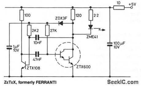
The transmitter consists of an oscillator which drives a high output IR emitting diode. The oscillator is a sure start multivibrator circuit that provides an output of 15 to 1000 mark to space ratio at a frequency of 1 kHz. This large mark to space ratio allows the IR diode to be operated at a high peak current, provided by the ZTX600 Darlington transistor, to maximize the transmitter range. A decoupling network is included in the power supply lead to isolate it from any logic circuitry using the same 5-V power supply source. The transmitter supply current is approximately 65 mA. (View)
View full Circuit Diagram | Comments | Reading(0)
DATA___MULTIPLEXER_DECODER
Published:2009/7/7 5:30:00 Author:May
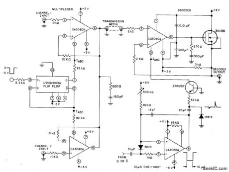
CD4013A flip-flop switches channel opamps alternately to transmission line under control of -5 V clock pulses for multiplexing of inputs to line, Any number of input channels can be added by ex tending circuit. At receiving end, one CA3080A variable opamp is used as mono MVBR to provide 10μs delay for input signal to settle before being sampled by sample-and-hold decoder. Either output of flip-flop can be used to trigger MVBR,- Circuit Ideas for RCA Linear ICs, RCA Solid State Division, Somerville, NJ, 1977, p 15. (View)
View full Circuit Diagram | Comments | Reading(1241)
0_10VDC_TO_0_10_kHz
Published:2009/7/7 5:03:00 Author:May
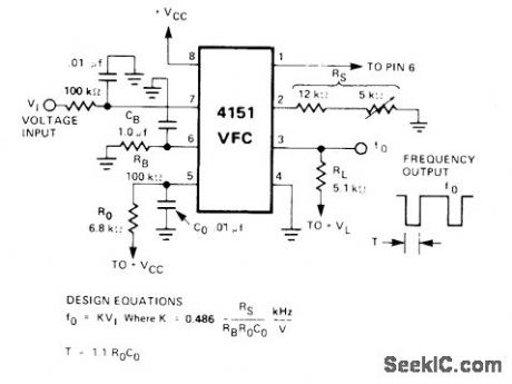
Single-supply voltage-to-frequency convener produces square-wave output at frequency varying linearly with input voltage. Linearity error is typically only 1%. For values shown, response time for step change of input from 0 to +10V is 135 ms. Uses Raytheon 4151 converter. Supply can be 15 V.- Linear Integrated Circuit Data Book, Raytheon Semi-conductor Division, Mountain View, CA, 1978, p7-38. (View)
View full Circuit Diagram | Comments | Reading(1153)
POSITIVE_TO_NEGATIVE_CONVERTER
Published:2009/7/7 4:29:00 Author:May
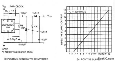

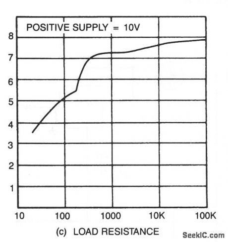
The transformerless dc-dc converter derives a negative supply voltage from a positive. As a bonus, the circuit also generates a clock signal. The negative output voltage tracks the dc-input voltage linearity (a), but its magnitude is about 3 V lower.Application of a 500- Ω load, (b), causes 10% change from the no-load value. (View)
View full Circuit Diagram | Comments | Reading(1211)
RS_232_TO_CMOS_LINE_RECEIVER
Published:2009/7/7 2:40:00 Author:May
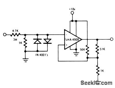
This RS-232 type line receiver to drive CMOS logic uses a Schmitt-trigger feedback network to give about 1-V input hysteresis for added noise immunity. A possible problem in an interface which connects two pieces of equipment, each plugged into a different ac receptacle, is that the power line voltage might appear at the receiver input when the interface connection is made or broken. The two diodes and a 3-W input resistor will protect the inputs under these conditions.
(View)
View full Circuit Diagram | Comments | Reading(1105)
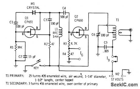
1_4_W_CW_TRANSMITTER
Published:2009/7/7 2:35:00 Author:May

Low-power two-stage FET transmitter for 80-meter amateur band uses Pierce crystal oscillator that requires no output resonant ci.rcuit. DC milliammeter can be connected across 150-ohm resistor in gate circuit of second transistor to indicate strength of oscillator output signal, Resonant circuit of RF amplifier Q2 uses toroid L2 (56turns No, 24 enamel 13/16-in Permacor 57-1541 core) and two series-connected trimmers. Milliam-meter is connected across C8 when level of BF output voltage js to be measured.-E. M. Noll, FET Principles, Experiments, and Projects, Howard W. Sams, Indianapolis, IN, 2nd Ed., 1975,p 204-207. (View)
View full Circuit Diagram | Comments | Reading(2598)
ONE_OF_EIGHT_CHANNEL_TRANSMISSION_SYSTEM
Published:2009/7/7 2:35:00 Author:May
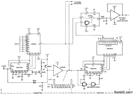
View full Circuit Diagram | Comments | Reading(1023)
100_W_AT_432_MHz
Published:2009/7/7 2:08:00 Author:May

Two-transistor 100-W PEP solid-state linear amplifier can be used for SSB activity in satellite relay service or for linear, CW, or FM service. Circuit uses Motorola MRF30628-V 60-W 225-400 MHz power tran-sistors in narrow-band parallel amplifier oper-ating in class AB linear mode. Drive level is about 10 W PEP. Article covers construction and tune-up.-R. K. Olsen, 100-Watt Solid-State Power Amplifier for 432 MHz, Ham Fladio, Sept.1975, p 36-43. (View)
View full Circuit Diagram | Comments | Reading(1424)
5_W_FET_TRANSMITTER
Published:2009/7/6 23:41:00 Author:May
Vaiues shown give operation in 40-meter amateur band. Drain of resonant tank circuit.-E. M. Noll, FET Principles, Experiments, and Projects, Howard W.Sams, Indianapolis, IN, 2nd Ed., 1975, p 188-power FET Q2 is connected to tap on primary of 189. (View)
View full Circuit Diagram | Comments | Reading(1229)
PCM_FOR_MICROWAVE_TRANSMITTER
Published:2009/7/6 23:21:00 Author:May
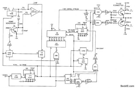
Modern pulse-code modulator can be used for experimentation above lowest legal frequency of 2.3 61ih, such as for satellite and moonbounce communication. Single voice channel is en-coded by using CMOS technology having low power consumption, good noise immunity, and moderate cost. Audio is sampled 10,000 times per second for conversion to 7-pulse code plus synchronizing bit, for 123 levels of encoding frequencies up to 5 kHz, When 10-kHz sampling spike (derived from external 1.28-MHz oscillator by frequency divider U10 and mono U11) arrives at pin 13 of transmission gate U1, AF voltage of pin 1 appears at pin 2.470-pF capacitor charges to this voltage and holds charge until next sample. This voltage is compared by U2 to linear ramp started by Q1 at sampling instant. When ramp voltage exceeds sampled voltage, U2 triggers, setting flip-flop U3 and resetting ramp generator to -5 V. Atsame time, binary counter U9 is stopped by reset flip-flop U15A, and binary equivalent of sample appears at pins 3, 4, 5, 6, 9, 11, and 12 of U9. Remainder of circuit converts bits to serial form for transmission. Article explains circuit operation in detail and gives corresponding decoder circuit for receiver.-V. Biancomano, A Prototype Pulse-Code Modulation System QST, Jan. 1977, p 24.-29. (View)
View full Circuit Diagram | Comments | Reading(4261)
CARRIER_CURRENT_AM_RECEIVER
Published:2009/7/6 20:49:00 Author:May

The AM Tuned Radio Frequency (TRF) receiver, has a sensitivity of about 1 mV at the input for an audio output of 1/2 W. Capacitor C22 couples audio signals from the power line to the PC board-it must be rated at 600 Vdc. R8 will cause Fl to blow, if C22 shorts. The signal from C22 goes to a tuned network (Ct through C5, L1, and L2) that has a 20-kHz bandwidth, which allows only the desired signal to pass through.
IC1 is again block i-f chip that has AGC capability and approximately 60 dB of gain. Components C8, C9, and L3, which are placed across the output of IC1, are broadly resonant around 280 kHz. C10 couples rf to detector-diode D1, which is used as an envelope detector.
The detector output is taken from C14,which sets the upper frequency limit at about 10 kHz or so.By reducing the value of C14, high frequency response can be obtatned. The detector output is connected to an external jack. Audio components are fed to audio-gain control R6, through C16 to IC2, an audio amplifier. C18 couples up to 1/2 watt of audio to an external speaker. The kit is available from North Country Radio, P.0. Box 53,Wykagyl Station, NY 10804. (View)
View full Circuit Diagram | Comments | Reading(2058)
CARRIER_CURRENT_FM_RECEIVER
Published:2009/7/6 20:45:00 Author:May
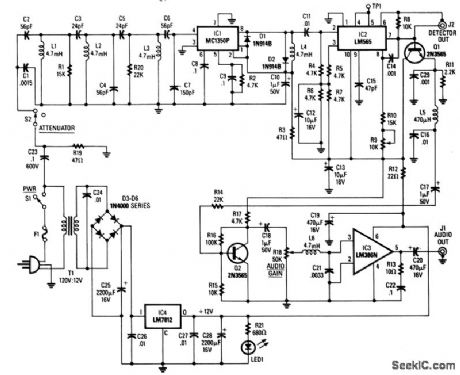
Input signals from the power line are coupled through C23 and R19 to the input filter network. C23 must be rated at 600 volts. Switch S2 is used as an attenuator. Components C2 through C7, L1 through L3, R1, and R20 form a triple-tuned bandpass filter having a passband from 220-340 kHz. Signals from the filter are fed to an MC1350P gain block IC, which is used as a tuned rf amplifier.
IC2, the LM565 PLL, is used as an FM demodulator. Pins 8 and 9 are connected to an internal VCO and components R9, R10, and C15 set the VCO's free running frequency. The VCO signal and the input signal from pin 2 are compared in the phase detector. The output from the phase detector is internally amplified, and then appears at pin 7. The output at pin 7 is a replica of the original modulation on the FM input signal to the receiver; the output at pin 7 is therefore the recovered audio. C17 and R14 couple audio to the base of Q2, which, in conjunction with R15, RIG, R17, and C18, form an audio amplifier that brings the recovered audio up to around 1 V peak-to-peak. The signal is then fed into an LM386N audio amplifier, which can deliver up to 1/2 W of audio, coupled via C20, to any standard 8- Ω external speaker. The kit is available from North Country Radio, P.O. Box 53, Wykagyl Station, NY 10804.
(View)
View full Circuit Diagram | Comments | Reading(2372)
REMOTE_SENSOR_LOOP_TRANSMITTER
Published:2009/7/6 8:49:00 Author:May
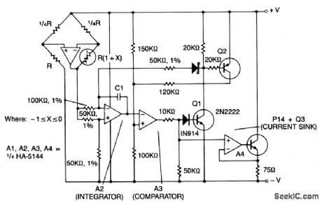
This circuit shows amplifier A1 as a sensor amplifier in a bridge configuration. Amplifiers A2 and A3 are configured as a voltage to frequency converter and A4 is used as the transmitter. This entire sensor/ transmitter can be powered directly from a 4 to 20 mA current loop.
The bridge configuration produces a linear output with respect to the changes in resistance of the sensor. The voltage at the output of Al causes the integrator output A2 to ramp down until it crosses the comparator threshold voltage of A3. A3 turns on Q1 and Q2. A1 causes the output of A2 to ramp up at a rate nearly equal to its negative slope, while Q2 provides hysteresis for the comparator. In addition, Q1 and Q2 help eliminate changes in power supply loop voltage. Amplifier A4 and Q3 are configured as a constant current sink which turns on when the comparator current increases. The resulting increase in loop current transmits the frequency of the V/F converter back to the control circuitry.
(View)
View full Circuit Diagram | Comments | Reading(1072)
ABSOLUTE_VALUE_RECTIFIER
Published:2009/7/6 6:46:00 Author:May
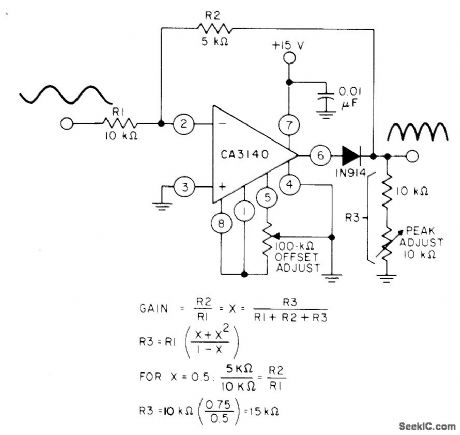
Use of CA3140 bipolar MOS opamp in inverting gain configuration give symmetrical full-wave output when equality of design equations is satisfied. Bandwith for -3 dB is 290 kHz, and average DC output is 3.2V for 20V p-p input.- Circuit Ideas for RCA linear ICs, RCA Solid State Division, Somerville, NJ, 1977, p 18. (View)
View full Circuit Diagram | Comments | Reading(1206)
100_kHz_BUFFERED_RECTIFIER
Published:2009/7/6 6:34:00 Author:May
High-speed 110 voltage follower is used within feedback loop of A1 to maintain low output impedance for precision half-wave rectifier, When input signal is positive, D1 and R4 rectify signal and A2 follows this signal. On opposite alternations, D1 is off and feedback loop of A2 is closed through D2 so output terminal is maintained at low impedance. For opposite output polarity, reverse diode connections.-W. G. Jung, IC Op-Amp Cookbook, Howard W. Sams, Indianapolis, IN, 1974, p 192. (View)
View full Circuit Diagram | Comments | Reading(1017)
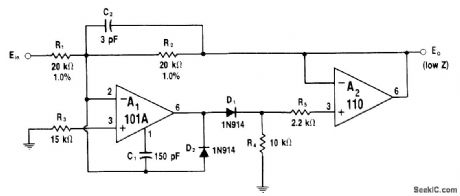
100_kHz_FULL_WAVE_RECTIFIER
Published:2009/7/6 6:19:00 Author:May
Feed-for-ward connection of opamps gives high-speed full-wave rectification of signals up to 100 kHz for measurement and analysis.-W. G. Jung, IC Op-Amp Cookbook, Howard W. Sams, Indianapolis, IN, 1974, p 193-194. (View)
View full Circuit Diagram | Comments | Reading(1272)
LIGHT_BEAM_RECEIVER
Published:2009/7/6 6:12:00 Author:May
Converts amplitude-modulated light beam back to audio signal for driving transistor radio earphone having resistance of 500-1000 ohms. Miniature 8-ohm loud-speaker can be used by adding output trans-former such as Radio Shack 273-1380. Gain of opamp is controlled by R3, which can be trimmer resistor or pot. Designed for use with transmitter providing amplitude modulation of LED, for short-range voice communication.-F. M. Mims, Optoelectronic Projects, Vol. 1, Radio Shack, Fort Worth, TX, 1977, 2nd Ed., p 44-54. (View)
View full Circuit Diagram | Comments | Reading(1385)
| Pages:16/32 1234567891011121314151617181920Under 20 |
Circuit Categories
power supply circuit
Amplifier Circuit
Basic Circuit
LED and Light Circuit
Sensor Circuit
Signal Processing
Electrical Equipment Circuit
Control Circuit
Remote Control Circuit
A/D-D/A Converter Circuit
Audio Circuit
Measuring and Test Circuit
Communication Circuit
Computer-Related Circuit
555 Circuit
Automotive Circuit
Repairing Circuit