
Control Circuit
Index 55
Hearing aids circuit
Published:2012/10/11 2:26:00 Author:muriel
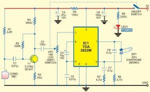
This low-cost, general-purpose electronic hearing aids works off 3V DC (2×1.5V battery). Transistor T1 and associated components form the audio signal preamplifier for the acoustic signals picked up by the condenser microphone and converted into corresponding electrical signals.The medium-power amplifier section is wired around popular audio amplifier IC TDA2822M (not TDA2822). This IC, specially designed for portable low-power applications, is readily available in 8-pin mini DIP package. Here the IC is wired in bridge configuration to drive the 32-ohm general-purpose monophonic earphone.
The audio output of this hearing aid circuit is 10 to 15 mW and the quiescent current drain is below 1 mA. The circuit can be easily assembled on a veroboard. For easy assembling and maintenance, use an 8-pin DIP IC socket for TDA2822M.
Hearing aids circuit wiring diagram
(View)
View full Circuit Diagram | Comments | Reading(1603)
Stereo switch circuit
Published:2012/10/11 2:21:00 Author:muriel | Keyword: Stereo switch
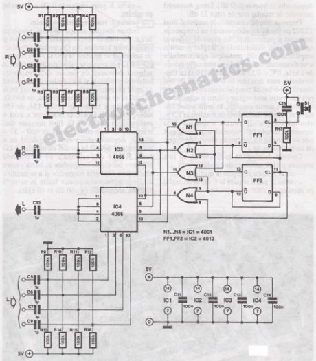
This stereo audio switch circuit allows that with only one switch to select one of the four stereo channels. The internal switching is made posible with CMOS components.
Each switch input includes a voltage divider to allow the switch to work in the linear zone of the characteristics, this ensures low audio signal distorsions.
Through the stereo switch circuit will flow a 1 mA current intensity at 5V. This voltage can be increased up to 15V.
Stereo audio switch circuit diagram
(View)
View full Circuit Diagram | Comments | Reading(1099)
The control alarm circuit with SGZ07 sound and light alarm integrated circuit
Published:2012/10/10 22:04:00 Author:Ecco | Keyword: control alarm , sound and light, alarm, integrated circuit
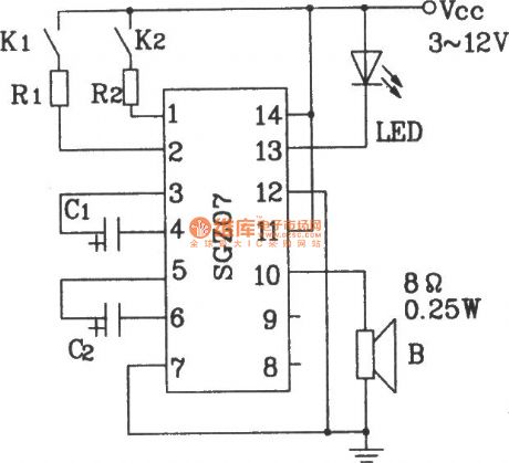
In the figure, the on-off of K1 the K2 allow the circuit to work in dual-band sound, light alarm circuit. If the R1, R2 of circuit are replaced by the corresponding thermistors ( measured value), it can realize the temperature control alarm circuit.
(View)
View full Circuit Diagram | Comments | Reading(1101)
ZKB8711 self-control alarm integrated circuit for thermostat automatic control alarm circuit
Published:2012/10/10 21:36:00 Author:Ecco | Keyword: self-control, alarm , integrated circuit, thermostat , automatic control , alarm
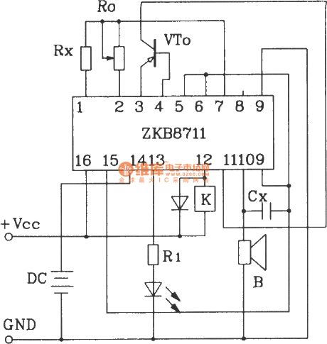
ZKB8711 can be used for temperature control, light control, rain control humidity control and hazardous gas detection alarm, the circuits with ZKB8711 have less external components, and they are easy to make.
(View)
View full Circuit Diagram | Comments | Reading(1626)
Automatic Gain Control – AGC circuit
Published:2012/10/10 1:52:00 Author:muriel | Keyword: Automatic, Gain Control
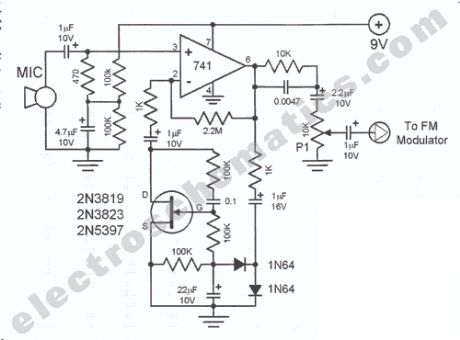
Automatic Gain Control or AGC is a circuit design which maintain the same level of amplification for sound or radio frequency. If the signal is too low the AGC circuit will increase (amplify) the level and if is to high will lower it to maintain a constant level as possible. The Automatic Gain Control principle is widely use in AM receivers and sometimes AGC is called an compressor-expander because it acts just like one.On the electroschematics.com site you can find some AGC schematics, just use the seach box.
Mic preamplifier with AGC schematic
(View)
View full Circuit Diagram | Comments | Reading(2594)
Electronic Locker Guard
Published:2012/10/10 1:46:00 Author:muriel | Keyword: Electronic Locker
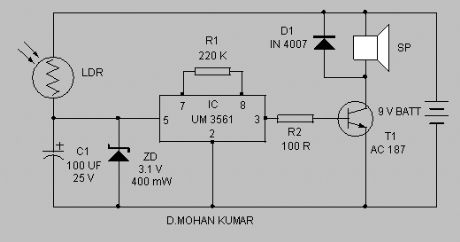
Protect your Locker or Briefcase from theft using this pocket sized gadget. It gives a loud police siren to catch attention.The circuit uses a single IC and a few discrete components. It works on the principle of light detection by LDR. When the unit is in dark, LDR cease to conduct and the alarm generator does not get power supply and it remains idle. When some one tries open the door of the locker, C1 charges via LDR. When the voltage in C1 raises to 3.1 volts, Zener conducts and gives power to IC UM 3561. It is a ROM IC that can generate different tones based on its pin connections. Here a police siren is selected by keeping pin6 floating. R1 determines the oscillation of IC. 220K (R1) is a must to give correct tone.C1 provides a lag of two minutes, so that the user gets sufficient time to disarm the unit.
Locker Guard Circuit Diagram
(View)
View full Circuit Diagram | Comments | Reading(1171)
Static Charge Monitor
Published:2012/10/9 2:41:00 Author:muriel | Keyword: Static Charge, Monitor
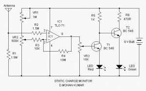
Here is a circuit that can sense the static electricity level in the atmosphere. It gives LED indications for both positive and negative atmosphere charges. The circuit uses a low noise JFET input Opamp TLO 71 to detect the atmospheric charge.The op amp has well matched high voltage JFET input device for low input offset voltage. The BIFET technology provides wide bandwidth and fast slew rate with two input bias currents. IC1 (TLO71) is designed as a voltage sensor cum signal amplifier. Its Non INV input is connected to the aerial (1 meter plastic wire) through R2. R1 maintains the input impedance of IC1 to make the input sensitivity normal.
VR1 and VR2 adjust the voltage level at the INV input of IC1. Resistor R3 and R4 determines the gain of the inverting amplifier and with the shown values it is 1000. That is, a difference of 1 milli volt at the input gives 1 volt output. Output from IC1 is used to switch on T1 and T2 at different output states.
When there is positive charge in the atmosphere, output of IC1 becomes high and T1 conducts to light Red LED. If the atmospheric charge is negative, output of IC1 remains low and T1 off. This causes T2 to conduct and Green LED lights. These states of LEDs change as the atmospheric charge changes. Adjust VR1 and VR2 for IC’s input sensitivity and VR3 for the threshold level of T1.Adjustments should be done in a sunny day so that atmospheric charge will be around 100 milli volts.
Static Charge Monitor Circuit Diagram
(View)
View full Circuit Diagram | Comments | Reading(1379)
Logic State Indicator
Published:2012/10/9 2:39:00 Author:muriel | Keyword: Logic State, Indicator
Here is a simple logic state indicator to test whether the output of digital IC is in logic 1 or 0. The Bicolor LED lights Green when the logic state is 1 and lights Red when the logic state is 0.The circuit uses only a few components and is based on the switching action of bipolar transistor. Normally the base of T1 is floating so that it will be off. This will allow T2 to conducts since its base gets bias through R2. The Red half of the bicolor LED lights indicating 0 logic. When the red probe connected to the base of T1 makes contact with a high signal output, T1 conducts and Green half of bicolor LED lights indicating logic 1. At the same time, T2 turns off and Red half of bicolor LED turns off. If the output is pulsating with alternate cycles, Red and Green LEDs lights alternately and if the transition is very fast both Red and Green LEDs lights giving yellow colour. The circuit can also be used as a continuity tester or Fuse tester.
Logic Stage Indicator Circuit Diagram
(View)
View full Circuit Diagram | Comments | Reading(769)
Peak indicator circuit schematic TLC272
Published:2012/10/9 2:37:00 Author:muriel | Keyword: Peak indicator
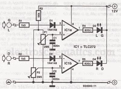
This peak indicator circuit signals thru 2 led’s the exceeding of a pre-estabilished value of any stereo audio channel.Signals from the 2 channels are rectified (monoalternance) with D1 and D2 and the resulted voltage is applied on OA IC TLC272 inversor entries.The peak indicator circuit can be used up to 20kHz frequency and the current consumption with led off is 0.25mA and with both leds on is 24mA.
Peak indicator circuit schematic
(View)
View full Circuit Diagram | Comments | Reading(1316)
LED Alarm Simulator circuit
Published:2012/10/9 2:37:00 Author:muriel | Keyword: LED Alarm, Simulator circuit
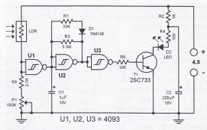
This circuit simulates an alarm to discourage thieves and it is originally designed to be used on bicycles but can be used for cars too. It blinks a LED on and off thus simulating a real alarm circuit.
The LED alarm electronic circuit consists of a square wave oscillator generating a 1 MHz signal with a pulse width of 10 milisecond. The LED lights u 10 miliseconds long. The circuit consumes 30 miliamperes when the LED lights and the average consumption is 300 microamperes.To switch off the circuit automatically it has a built in LDR. When the LDR is exposed to light it becomes low ohmic and the output of U1 becomes 0. The oscillator stops and the LED turns off. The light sensitivity of the circuit is set with the potentiometer P1.
When there is no light falling on the LDR, the input of U1 is connected to the ground and its output becomes “1″ thereby starting the oscillator which drives the LED to blink. If the circuit is powered with a 4.5 volts battery that has a 2 Ah capacity, it will work for aroung 1.5 years.
LED flashing alarm circuit diagram
(View)
View full Circuit Diagram | Comments | Reading(872)
Solar Charger Monitor circuit
Published:2012/10/9 2:31:00 Author:muriel | Keyword: Solar Charger, Monitor
This add on circuit can be attached to the solar charger to see whether the battery is charging or not. It lights a Red LED to indicate that the battery is not accepting charge. It gives a warning indication if there is any loose connection with the charger and battery.The Solar charger monitor circuit uses two PNP transistors T1 and T2 to give a warning indication if there is any loose connection with the charger and battery. If the connection is intact and current is flowing into the battery, diodes D2 and D3 forward bias and drops around 1.2 volts. This forward voltage drop across the diodes causes T2 to conducts. The collector current from T2 keeps the base of T1 high and it remains off. Red LED connected to the emitter of T1 remains off indicating that current is flowing to the battery and the connections are intact. When there is any break in the connecting cables or any loose contacts in the terminals, no more current passes and D2 and D3 reverse biases. This turns off T2 and T1 conducts .LED lights indicating that battery is not getting charging current.
Solar Charger Monitor Circuit Diagram
(View)
View full Circuit Diagram | Comments | Reading(925)
Digital Volume Control Circuit
Published:2012/10/9 2:30:00 Author:muriel | Keyword: Digital, Volume Control
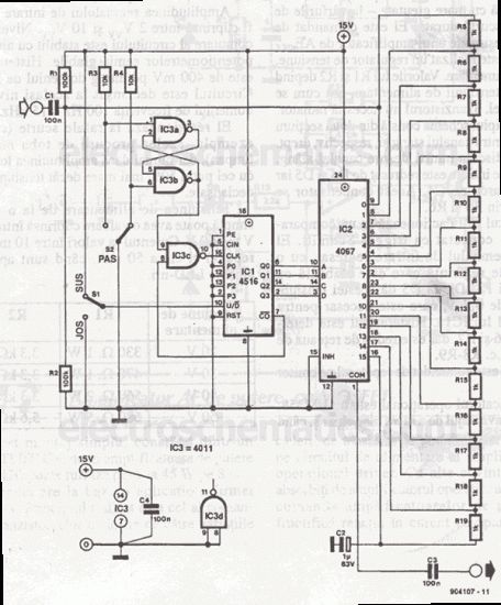
The heart of this digital volume controller DVC circuit is IC2 4067, 16-channel analog multiplexer.Because the 1kΩ has been connected between every input and output, the multiplexer can act like a potentiometer. The total resistance is 15kΩ . You can use different values for the resistor to obtain a different characteristic. The current consumption is 1mA.
Digital Volume Control Circuit Diagram
(View)
View full Circuit Diagram | Comments | Reading(2956)
Temperature indicator circuit
Published:2012/10/9 2:30:00 Author:muriel | Keyword: Temperature indicator
The multimeter is a measurement device most used by engineers and we use it in this temperature indicator circuit schematic. The temperature sensor is LM335 wich has a linear characteristic of 10mV / K . In the production process this electronic device is calibrated so can provide 2.73V at 00C.LM336 is used as a very precise 2.5V Zener diode; CA3040 amplification can be adjust between 1.08 and 1.10 times thru P1. This temperature measurement circuit can be used for Fahrenheit measurements, in this case the freezing point is adjusted at 320F. At 2120F, P2 is adjusted to obtain 0.9V at output.So 10F correspond to 5mV. The total current consumption is 10mA.
Temperature sensor circuit diagram
(View)
View full Circuit Diagram | Comments | Reading(820)
Delay On Circuit
Published:2012/10/9 2:29:00 Author:muriel | Keyword: Delay On Circuit
Protect your LCD or Plasma TV with this tiny delay on circuit. The SMPS based power supply of these modern electronic devices is vulnerable to spikes in the mains line so it gives a time delay of one minute before applying power to the device. This prevents deleterious effects due to inrush current and spurious spikes at power on.Inrush current at power on or power resumes after a power failure can cause unexpected damage in SMPS based power supply of electronic devices. The spurious spike in the power supply when power resumes is due to heavy magnetic flux in the distribution transformer in the mains network. If a short delay is provided, such damages can be avoided. The circuit descried here is intended for this purpose. It gives power to the device only after one to two minutes of delay after the power is switched on. The circuit is a zener controlled switch.
Capacitor C1 charges through R1 and VR. When the voltage in C1 rises above 3.1 volts, zener conducts to trigger T1. The relay connected to the collector of T1 energizes and power will be available through the common and Normally Open contacts of the relay. Relay remains latched as long as the voltage level in the mains is normal. Capacitor C2 keeps the base bias of T1 steady so that relay clicking can be avoided. Diode D1 prevents back e.m.f when T1 switches off. Red LED indicates the Relay On status. Delay time depends on the value of C1.
Delay-On Circuit Diagram
Power to the circuit can be derived from a standard 12 volt transformer with rectifier and smoothing capacitor. Use a socket to connect the TV as shown.
(View)
View full Circuit Diagram | Comments | Reading(850)
Battery Monitor Circuit
Published:2012/10/9 2:28:00 Author:muriel | Keyword: Battery, Monitor
Here is a simple Battery Monitor circuit for a quick check of 12 volt Lead-Acid Battery. Battery charge should be constantly monitored to increase the life of the battery. Overcharge as well as under charge will reduce the battery life. The terminal voltage of the Lead Acid battery should be with in the range of 12.5 to 13.5 volts. If the battery voltage reduces below 10 volts for long period, battery will not accept any charging current. Similarly if the terminal voltage exceeds above 14 volts, battery will be destroyed.The circuit is a Zener controlled transistor switch lighting three LEDs Red, Green and Yellow to show battery states like Low, Normal and High. When the battery voltage is less than 11 volts, Zener diodes ZD1 and ZD2 cease to conduct and Red LED only lights indicating low battery condition. If the voltage is between 12 volt and 14 volts, Zener diode ZD1 forward bias and T1 conducts. The Green LED connected to the collector of T1 lights indicating normal voltage. If the battery voltage exceeds 15 volts, Zener diode ZD2 also conducts and T2 forward bias. This lights Yellow LED indicating over charge. Thus the following indications can be obtained
Red Low voltageGreen Normal voltageGreen and Yellow Over voltage
Battery Monitor Circuit Diagram
(View)
View full Circuit Diagram | Comments | Reading(716)
Light Sensitive Switch Circuit
Published:2012/10/8 2:49:00 Author:muriel | Keyword: Light Sensitive, Switch
There are a wide range of applications for light sensitive switches: lighting, entrance door, automatic staircase, automatic opening of doors to the action of a ray of light, alarm systems, etc… Many of us are familiar with photosensitive switches made with a single transistor that is controlled by a photoresistor placed between the base and the recharger, depending on what is desired: normal functioning “closed” or normal “open” the switch.This configuration allows easy installation more complex, involving the use of operational amplifiers, especially those of type 741, which are very cheap. Another way to optodetect, less known, uses a bridge assembly, which operates on the principle that when the current is zero diagonal axle, means that the bridge is balanced.
This last principle is used in the sensitive switch installation you will be presented next. Photocell is placed in a bridge circuit and a comparator is used as detector bridge balanced. The comparator’s output control thyristor through a transistor. In this circuit, protective measures must be taken because it is isolated from the network.
Light Switch Circuit Diagram
Power supply circuit is taken from the bridge rectifier D1…D4 is filtered and stabilized by R1, C1, and D5. The bridge circuit is difficult to identify in the given diagram, but it is made of R2 ….. R4, P1 and photoresist (LDR). IC1 is used in the comparator configuration and power level will be about 1.8 V when potential entry vice versa (negative) exceed that of the entry non vice versa. Resistance R5 conducts a hysteresis of about 1V to prevent thyristor to oscillate at T1 and threshold lighting.
Switching point of the light sensitive switch may be adjusted from P1. With the potentiometer set the minimum (minimal resistance) lamp will light a crepuscular light. If you want more flexibility, replace P1 with one that has a value of 1 MΩ. If desired operation reverse position in the scheme of the photoresistor can be changed with the group P1/R4. LA1 lamp will be extinguished, in this case, after dark.
Some practical advice: if you want to use higher power lamps then diodes D1 …. D4 need to be replaced with other type 1N5404 and thyristor TH1 will be equipped with a heat sink. With these changes, the circuit can control currents up to 3A.
Maximum gate for TH1 is 250 µA, which means that you must use a very sensitive thyristor. It can use any type of photoresistor. Remember precautions to be taken due to lack of isolation mounting over the network. It is important that the entire circuit to be protected in a plastic box, of any shape, provided with a hole in the upper side, in order to allow to the photoresistance “to see”. Assure that the entry cable and the exit cable are fixed. This precautions will assure you from accidents.
Light Sensitive Switch PCB Layout
(View)
View full Circuit Diagram | Comments | Reading(1269)
LASER Door Alarm circuit
Published:2012/10/8 2:49:00 Author:muriel | Keyword: LASER, Door, Alarm
This laser door alarm is based on the interruption of Laser beam. A low cost Laser pointer is used as the source of light beam. When somebody breaks the laser path, the alarm will be generated for few seconds.
Laser Door Alarm Circuit Diagram
The laser door alarm circuit has two sections. The laser transmitter is a laser pointer readily available. It should be powered with 3 volt DC supply and fixed on one side of the door frame. The receiver has a Phototransistor at the front end. L14F1 NPN Darlington phototransistor is used as the laser sensor. IC1 is used as a voltage comparator with its inverting input tied to a potential divider R2-R3. So that the inverting input is kept at half supply voltage.
The non inverting input receives a variable voltage based on the conduction of T1. The receiver should be fixed on the opposite door frame and should be properly aligned to the laser beam. Normally the laser beam illuminates the face of phototransistor and it conducts. This keeps the voltage at pin 3 lower than pin 2 of IC1.
As a result, output of comparator remains low. LED and Buzzer remain off in this state. When a person crosses the door, laser beam breaks and T1 cease to conduct. Collector voltage of T1 rises and voltage at pin 3 of comparator increases and its output becomes high. This activates LED and buzzer. Capacitor C1 keeps the base of T2 high for few seconds even after the output of IC1 becomes low again. C2 gives current to the buzzer for few seconds even after T2 turns off.
Caution: This circuit uses harmful laser rays. Do not look into the Laser pointer. It should not be placed in places accessible to children.
(View)
View full Circuit Diagram | Comments | Reading(1419)
PC Fan Controller circuit
Published:2012/10/8 2:48:00 Author:muriel | Keyword: PC Fan, Controller
This PC fan controller circuit is designed with discrete components and is used to control 12 V fans that have a current consumption lower than 200 mA. With the components values presented in the circuit diagram, the voltage won’t drop below 7 V. If the fan won’t start at 250C then temporarily replace the temperature sensor KTY10 with a 1.8 kΩ resistor and reduce the value of R7. If the PC fan has a speed too high then increase the R7 value.T1 and T2 transistors compare the fixed potentional from R3-R4 common point with the temperature dependent potentional of R1-R2 common point. It may be useful to connect a 25 kΩ potentiometer instead of R2 and to adjust it until the PC fan is at the correct speed and to measure its resistance and then replace it with a fix resistor with the same value.
PC Fan Controller Circuit Diagram
Place the temperature sensor in the warm air of the fan. When the PC is connected the speed rotation of the fan will be pretty high because of C1 but will decrease at a minimum value. Measure with a thermometer the air temperature close to the sensor. When the temperature reaches 350C the pc fan controller circuit will start to work. If this won’t happen modify the value of R2 or adjust a potentiometer placed instead of R2. When the temperature increases so will the rotation speed of the PC fan. The maximum speed will be lower than the one obtained without the control circuit. (View)
View full Circuit Diagram | Comments | Reading(1293)
Electronic Dice circuit
Published:2012/10/8 2:44:00 Author:muriel | Keyword: Electronic Dice
With this electronic dice the result is displayed with LEDs that are placed so every dice face is shown. In the circuit diagram, IC 4022 is used to count to 6 in which only one output can get “1″ state.A diode matrix (D1..D8) serve as decoding the output signals of the counter so that the LEDs are controlled by two buffer transistors and series resistance.Integrated circuit outputs only support a reduced load, so in the transistor’s base are connected the limiting resistances. As a clock generator it can be used any generator with rectangular pulses whose amplitude corresponds to the IC’s supply voltage. The 4022 clock input impedance is 1012Ω.
Electronic Dice Circuit Diagram
(View)
View full Circuit Diagram | Comments | Reading(746)
Car DC Adapter circuit
Published:2012/10/8 2:43:00 Author:muriel | Keyword: Car, DC Adapter
Here is a DC adapter to charge Mobile phone or play a Music system using the power from car battery. The adapter will provide 4.7 volt regulated DC from the 13.5 volt DC power of the car battery. The circuit is basically a DC to DC converter with voltage and current regulation. The 13.5 volt DC from the car battery is given to the collector and base of T1. R1 restricts the base current of T1 to a safer level so that output will be current regulated. T1 is an NPN Darlington transistor so that its high gain gives maximum output current. Diode D1 protects the circuit from accidental polarity reversal during connections. By changing the value of ZD, it is possible to get required output voltage. Here the 4.7 volt zener gives regulated 4.7 volts for charging a mobile phone. The adapter can be plugged into the cigarette lighter outlet of the car dash board.It is better to give heat sinking to T1 to dissipate heat.
Car DC Adapter Circuit Diagram
TIP 122 Darlington Transistor
(View)
View full Circuit Diagram | Comments | Reading(957)
| Pages:55/312 At 204142434445464748495051525354555657585960Under 20 |
Circuit Categories
power supply circuit
Amplifier Circuit
Basic Circuit
LED and Light Circuit
Sensor Circuit
Signal Processing
Electrical Equipment Circuit
Control Circuit
Remote Control Circuit
A/D-D/A Converter Circuit
Audio Circuit
Measuring and Test Circuit
Communication Circuit
Computer-Related Circuit
555 Circuit
Automotive Circuit
Repairing Circuit