
Control Circuit
Index 54
PIC Digital Clock Timer
Published:2012/10/22 1:18:00 Author:muriel | Keyword: PIC , Digital Clock, Timer
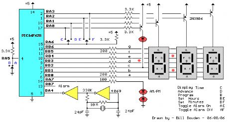
This clock timer uses a PIC16F628 microcontroller to display 3 and 1/2 digit time and control an external load. The clock includes a calendar with leap year and optional daylight savings adjustments. The timer output can be set from 1 to 59 minutes and manually switched on and off. The clock also has a correction feature that allows an additional second to be added every so many hours to compensate for a slightly slow running oscillator. The oscillator uses a common 32.768 KHz watch crystal and the frequency can be adjusted slightly with the 24pF capacitor on the right side of the crystal. (View)
View full Circuit Diagram | Comments | Reading(3232)
28 LED Clock Timer
Published:2012/10/22 1:09:00 Author:muriel | Keyword: 28 LED, Clock Timer
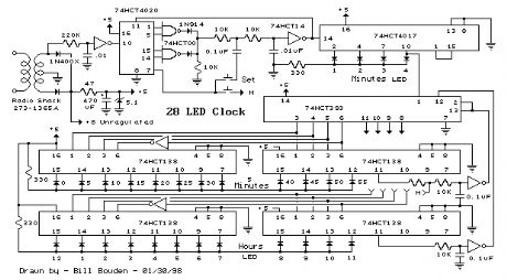
This is a programmable clock timer circuit that uses individual LEDs to indicate hours and minutes. 12 LEDs can be arranged in a circle to represent the 12 hours of a clock face and an additional 12 LEDs can be arranged in an outer circle to indicate 5 minute intervals within the hour. 4 additional LEDs are used to indicate 1 to 4 minutes of time within each 5 minute interval. The circuit is powered from a small 12.6 volt center tapped line transformer and the 60 cycle line frequency is used for the time base. The transformer is connected in a full wave, center tapped configuration which produces about 8.5 volts unregulated DC. A 47 ohm resistor and 5.1 volt, 1 watt zener regulate the supply for the 74HCT circuits. A 14 stage 74HCT4020 binary counter and two NAND gates are used to divide the line frequency by 3600 producing a one minute pulse which is used to reset the counter and advance the 4017 decade counter. The decade counter counts the minutes from 0 to 4 and resets on the fifth count or every 5 minutes which advances one section of a dual 4 bit binary counter (74HCT393). The 4 bits of this counter are then decoded into one of 12 outputs by two 74HCT138 (3 line to 8 line) decoder circuits. The most significant bit is used in conjunction with an inverter to select the appropriate decoder. During the first eight counts, the low state of the MSB is inverted to supply a high level to enable the decoder that drives the first 8 LEDs. During counts 9 to 12, the MSB will be high and will select the decoder that drives the remaining 4 LEDs while disabling the other decoder. The decoded outputs are low when selected and the 12 LEDs are connected common anode with a 330 ohm current limiting resistor to the +5 volt supply. The 5th output of the second decoder (pin 11) is used to reset the binary counter so that it counts to 11 and then resets to zero on the 12th count. A high reset level is required for the 393 counters, so the low output from the last decoder stage (pin 11) is inverted with one section of a 74HCT14 hex Schmitt trigger inverter circuit. A 10K resistor and 0.1uF cap are used to extend the reset time, ensuring the counter receives a reset signal which is much longer than the minimum time required. The reset signal is also connected to the clock input (pin 13) of the second 4 bit counter (1/2 74HCT393) which advances the hour LEDs and resets on the 12th hour in a similar manner. Setting the correct time is accomplished with two manual push buttons which feed the Q4 stage (pin 7) of the 4020 counter to the minute and hour reset circuits which advance the counters at 3.75 counts per second. A slower rate can be obtained by using the Q5 or Q6 stages. For test purposes, you can use Q1 (pin 9) which will advance the minutes at 30 per second. The time interval circuit (shown below the clock) consists of a SET/RESET flipflop made from the two remaining NAND gates (74HCT00). The desired time interval is programmed by connecting the anodes of the six diodes labeled start, stop and AM/PM to the appropriate decoder outputs. For example, to turn the relay on at 7:05AM and turn it off at 8:05AM, you would connect one of the diodes from the start section to the cathode of the LED that represents 7 hours, the second diode to the LED cathode that represents 5 minutes and the third diode to the AM line of the CD4013. The stop time is programmed in the same manner. Two additional push buttons are used to manually open and close the relay. The low start and stop signals at the common cathode connections are capacitively coupled to the NAND gates so that the manual push buttons can override the 5 minute time duration. That way, you can immediately reset the relay without waiting 5 minutes for the start signal to go away. The two power supply rectifier diodes are 1N400X variety and the switching diodes are 1N914 or 4148s but any general purpose diodes can be used. 0.1 uF caps (not shown on schematic) may be needed near the power pins of each IC. All parts should be available from Radio Shack with the exception of the 74HCT4017 decade counter which I didn't see listed. You can use either 74HC or 74HCT parts, the only difference between the two is that the input switching levels of the HCT devices are compatible with worst case TTL logic outputs. The HC device inputs are set at 50% of Vcc, so they may not work when driven from marginal TTL logic outputs. You can use a regular 4017 in place of the 74HCT4017 but the output current will much lower (less than 1 mA) and 4 additional transistors will be required to drive the LEDs. Without the buffer transistors, you can use a 10K resistor in place of the 330 and the LEDs will be visible, but very dim. Using the 4017 to drive LEDs with transistor buffers is shown in the 10 Channel LED Sequencer at the top of this page. (View)
View full Circuit Diagram | Comments | Reading(1030)
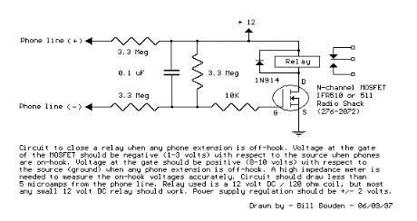
Telephone In-Use Relay Controller
Published:2012/10/19 0:52:00 Author:muriel | Keyword: Telephone, In-Use Relay, Controller
View full Circuit Diagram | Comments | Reading(692)
Do-it-yourself phone dialer security system
Published:2012/10/19 0:46:00 Author:muriel | Keyword: Do-it-yourself phone, dialer security system
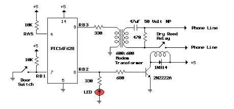
Do-it-yourself phone dialer security system calls your cell phone, office etc.whenever a door or window is opened, or panic button is pressed. Great Home Alarm.The circuit consists of a small PIC microcontroller, assembly program,and a few other parts to detect a switch closure from an open door, window,or manual push button and then dial the cell phone number, and transmit asteady tone to indicate the source of the call. The circuit uses the pulsedialing system to interrupt the line connection a number of times toindicate each digit. Pulse dialing (the oldest form of dialing) works byactually disconnecting or hanging up the phone line a number of timesto indicate each digit. For example, the digit 5 would be dialed bydisconnecting and reconnecting the line 5 times in short intervals ofabout 100mS. There is about a 1 second pause (with the line connected)between each digit. The timing is not critical and I was able to dial411 and connect to the local information service just using a momentarypush button switch in series with the phone line. (View)
View full Circuit Diagram | Comments | Reading(2047)
Generating Long Time Delays
Published:2012/10/18 22:58:00 Author:muriel | Keyword: Generating, Long Time , Delays
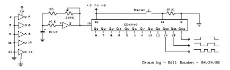
Generating long delays of several hours can be accomplished by using a low frequency oscillator and a binary counter as shown below. A single Schmitt Trigger inverter stage (1/6 of 74HC14) is used as a squarewave oscillator to produce a low frequency of about 0.5 Hertz. The 10K resistor in series with the input (pin 1) reduces the capacitor discharge current through the inverter input internal protection diodes if the circuit is suddenly disconnected from the supply. This resistor may not be needed but is a good idea to use.
The frequency is divided by two at each successive stage of the 12 stage binary counter (CD4040) which yields about 1 hour of time before the final stage (Q12) switches to a high state. Longer or shorter times can be obtained by adjusting the oscillator frequency or using different RC values. Each successive stage changes state when the preceding stage switches to a low state (0 volts), thus the frequency at each stage is one half the frequency of the stage before. Waveform diagrams are shown for the last 3 stages. To begin the delay cycle, the counter can be reset to zero by momentarily connecting the reset line (pin 11) to the positive supply. Timing accuracy will not be as good as with a crystal oscillator and may only be around 1 or 2% depending on the stability of the oscillator capacitor. (View)
View full Circuit Diagram | Comments | Reading(866)
1 Second Time Base From Crystal Oscillator
Published:2012/10/18 22:52:00 Author:muriel | Keyword: 1 Second Time, Crystal Oscillator
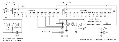
At 1 Mhz, the 330K resistor in the oscillator circuit will need to be reduced proportionally to about 15K. When the terminal count is reached, a 7 uS reset pulse is generated by the Schmitt Trigger inverter stage that follows the NAND gate. The 47K resistor and 470 picofarad capacitor sustain the output so that the counters are reliably reset to zero. This is less than one clock cycle at 50Khz and does not introduce an error but would amount to 7 cycles at 1 MHz which would cause the counters to lose 7 microseconds of time per second. It's not much of an error (7 parts in a million) but it would be there. The minimum reset pulse width for the 4040 CMOS counters is about 1.5 uS, so the reset pulse cannot be made much shorter. (View)
View full Circuit Diagram | Comments | Reading(1096)
1.5 Hour Lamp Fader (Sunset Lamp)
Published:2012/10/18 22:44:00 Author:muriel | Keyword: 1.5 Hour , Lamp Fader , Sunset Lamp
Similar to the one above, the sunset lamp comes on at full brightness and then slowly fades out over 1.5 hours time and stays off until power is recycled. (View)
View full Circuit Diagram | Comments | Reading(887)
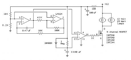
Automatic 12 Volt Lamp Fader
Published:2012/10/18 22:44:00 Author:muriel | Keyword: Automatic, 12 Volt, Lamp Fader
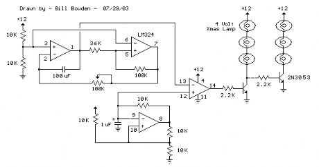
This circuit is similar to the Fading Red Eyes circuit (in the LED section) used to fade a pair of red LEDs. In this version, the lamps are faded by varying the duty cycle so that higher power incandescent lamps can be used without much power loss. The switching waveform is generated by comparing two linear ramps of different frequencies. The higher frequency ramp waveform (about 75 Hz.) is produced from one section of the LM324 quad op-amp wired as a Schmitt trigger oscillator. The lower frequency ramp controls the fading rate and is generated from the upper two op-amps similar to the fading eyes circuit. The two ramp waveforms at pins 9 and 1 are compared by the 4th op-amp which generates a varying duty cycle rectangular waveform to drive the output transistor. A second transistor is used to invert the waveform so that one group of lamps will fade as the other group brightens. The 2N3053 will handle up to 500 milliamps so you could connect 12 strings of 4 LEDs each (48 LEDs) with a 220 ohm resistor in series with each group of 4 LEDs. This would total about 250 milliamps. Or you can use three 4 volt, 200 mA Xmas tree bulbs in series. For higher power 12 volt automobile lamps, the transistor will need to be replaced with a MOSFET that can handle several amps of current. See the drawing below the schematic for possible hookups. (View)
View full Circuit Diagram | Comments | Reading(1028)
12 Volt Lamp Dimmer
Published:2012/10/18 22:43:00 Author:muriel | Keyword: 12 Volt, Lamp Dimmer
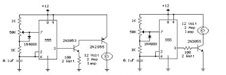
Here is a 12 volt / 2 amp lamp dimmer that can be used to dim a standard 25 watt automobile brake or backup bulb by controlling the duty cycle of a astable 555 timer oscillator. When the wiper of the potentiometer is at the uppermost position, the capacitor will charge quickly through both 1K resistors and the diode, producing a short positive interval and long negative interval which dims the lamp to near darkness. When the potentiometer wiper is at the lowermost position, the capacitor will charge through both 1K resistors and the 50K potentiometer and discharge through the lower 1K resistor, producing a long positive interval and short negative interval which brightens the lamp to near full intensity. The duty cycle of the 200 Hz square wave can be varied from approximately 5% to 95%. The two circuits below illustrate connecting the lamp to either the positive or negative side of the supply. (View)
View full Circuit Diagram | Comments | Reading(1079)
Reading Data From The Parallel Port
Published:2012/10/18 22:39:00 Author:muriel | Keyword: Parallel Port
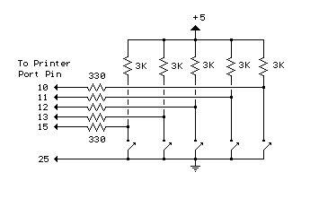
The diagram below shows 5 switches connected to the 5 input lines of the parallel port. An external 5 volt power supply is used to provide high logic levels to the input pins when the switches are open. Three 1.5 volt batteries in series can be used to obtain 4.5 volts which is close enough. The 330 ohm resistors in series with the port connections provide some protection in case a connection is made to the wrong pin. If you are sure of the connections, the 330 ohm resistors can be left out and the switches connected directly to the input pins. The negative side of the power supply should be connected to the ground point, or any pin from 18 to 25.
The following short QBasic program can be used to read the state of the switches. QBASIC.EXE can be found in the OLDMSDOS directory of the Windows 95/98 CD Rom. Note that there are three possible printer port address that correspond to LPT1, LPT2 and LPT3 and LPT1 is usually the one to use which is at address decimal 889. The program waits for the user to press the enter key before reading the state of the 5 input lines. The state of the 5 lines is received as a single 8 bit number between 0-255 which is stored as the value of (V). Each switch input represents a decimal value of 8,16,32,64 and 128 which correspond to pins 15,13,12,10 and 11. The last 3 bits (1,2 and 4) are not used and should return a high level, so the value received with all switches open should be 1+2+4+8+16+32+64=127. If a switch is closed and the input is at ground, the value will be 0 except for pin 11 which is inverted and yields a value of 128 and 0 when high, so the value received when all switches are closed should be 1+2+4+128=135. (View)
View full Circuit Diagram | Comments | Reading(1214)
Parallel Port Relay Interface
Published:2012/10/18 22:39:00 Author:muriel | Keyword: Parallel Port, Relay Interface
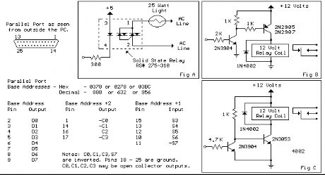
Below are three examples of controlling a relay from the PC's parallel printer port (LPT1 or LPT2). Figure A shows a solid state relay controlled by one of the parallel port data lines (D0-D7) using a 300 ohm resistor and 5 volt power source. The solid state relay will energize when a 0 is written to the data line. Figure B and C show mechanical relays controlled by two transistors. The relay in figure B is energized when a 1 is written to the data line and the relay in figure C is energized by writing a 0 to the line. In each of the three circuits, a common connection is made from the negative side of the power supply to one of the port ground pins (18-25).
There are three possible base addresses for the parallel port You may need to try all three base addresses to determine the correct address for the port you are using but LPT1 is usually at Hex 0378. The QBasic OUT command can be used to send data to the port. OUT, &H0378,0 sets D0-D7 low and OUT, &H378,255 sets D0-D7 high. The parallel port also provides four control lines (C0,C1,C2,C3) that can be set high or low by writing data to the base address+2 so if the base address is Hex 0378 then the address of the control latch would be Hex 037A. Note that three of the control bits are inverted so writing a 0 to the control latch will set C0,C1,C3 high and C2 low. (View)
View full Circuit Diagram | Comments | Reading(1795)
OpAmp Stall-Motor Switch Machine Drivers
Published:2012/10/18 3:33:00 Author:muriel | Keyword: OpAmp, Stall-Motor Switch, Machine Drivers
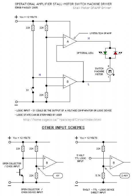
The circuits on this page are switch machine drivers that can be used to operate Stall-Motor type switch machine motors. The circuits use LM324 Quad or 358 Dual operational Amplifier chips to provide a PUSH-PULL output to reverse the polarity of the supply to the switch machine motors.
The drivers use direct control inputs such as switches or CMOS and TTL logic devices.
The advantage of this type of driver is low cost and, in the case of the 324, two drivers per package can be built. These operational amplifiers can only supply enough output current to drive one switch machine per driver. (View)
View full Circuit Diagram | Comments | Reading(1173)
CMOS SCHMITT TRIGGER IC
Published:2012/10/18 3:18:00 Author:muriel | Keyword: CMOS, SCHMITT , TRIGGER IC
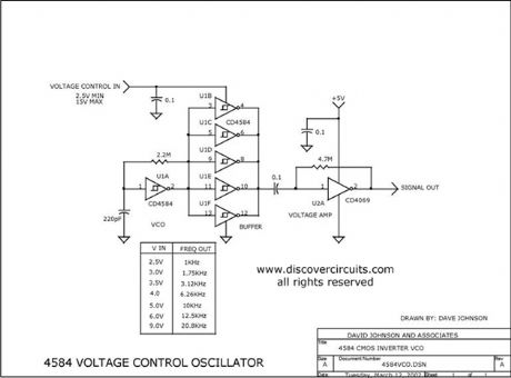
By changing the supply voltage fed to a classic 4584 Schmitt trigger type oscillator, the oscillator frequency can be changed over a range of 50:1. A 74HCU04 inverter is used at the output of the 4584 to maintain a constant TTL logic level signal. (View)
View full Circuit Diagram | Comments | Reading(2758)
Input current protection circuit diagram using INA321/322
Published:2012/10/17 21:14:00 Author:Ecco | Keyword: Input current , protection
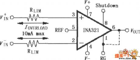
INA321/322 input end's interior has electrostatic discharge (ESD) protection diode, and the protection diode will get conduction when the input voltage exceeds the supply voltage 500mV, then RLIM will limit the input current ( 10mA ) to play a role in the protection circuit. Many input signals have limited streaming capabilities, at the time, the current limiting resistor RLIM can be ignored.
(View)
View full Circuit Diagram | Comments | Reading(802)
Digital Electronic Lock
Published:2012/10/17 22:24:00 Author:muriel | Keyword: Digital, Electronic Lock
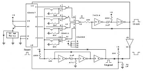
The digital lock shown below uses 4 common logic ICs to allow controlling a relay by entering a 4 digit number on a keypad. The first 4 outputs from the CD4017 decade counter (pins 3,2,4,7) are gated together with 4 digits from a keypad so that as the keys are depressed in the correct order, the counter will advance. As each correct key is pressed, a low level appears at the output of the dual NAND gate producing a high level at the output of the 8 input NAND at pin 13. The momentary high level from pin 13 activates a one shot circuit which applies an approximate 80 millisecond positive going pulse to the clock line (pin 14) of the decade counter which advances it one count on the rising edge. A second monostable, one shot circuit is used to generate an approximate 40 millisecond positive going pulse which is applied to the common point of the keypad so that the appropriate NAND gate will see two logic high levels when the correct key is pressed (one from the counter and the other from the key). The inverted clock pulse (negative going) at pin 12 of the 74C14 and the positive going keypad pulse at pin 6 are gated together using two diodes as an AND gate (shown in lower right corner). The output at the junction of the diodes will be positive in the event a wrong key is pressed and will reset the counter. When a correct key is pressed, outputs will be present from both monostable circuits (clock and keypad) causing the reset line to remain low and allowing the counter to advance. However, since the keypad pulse begins slightly before the clock, a 0.1uF capacitor is connected to the reset line to delay the reset until the inverted clock arrives. The values are not critical and various other timing schemes could be used but the clock signal should be slightly longer than the keypad pulse so that the clock signal can mask out the keypad and avoid resetting the counter in the event the clock pulse ends before the keypad pulse. The fifth output of the counter is on pin 10, so that after four correct key entries have been made, pin 10 will move to a high level and can be used to activate a relay, illuminate an LED, ect. At this point, the lock can be reset simply by pressing any key. The circuit can be extended with additional gates (one more CD4011) to accept up to a 8 digit code. The 4017 counting order is 3 2 4 7 10 1 5 6 9 11 so that the first 8 outputs are connected to the NAND gates and pin 9 would be used to drive the relay or light. The 4 additional NAND gate outputs would connect to the 4 remaining inputs of the CD4068 (pins 9,10,11,12). The circuit will operate from 3 to 12 volts on 4000 series CMOS but only 6 volts or less if 74HC parts are used. The circuit draws very little current (about 165 microamps) so it could be powered for several months on 4 AA batteries assuming only intermittent use of the relay.
(View)
View full Circuit Diagram | Comments | Reading(1016)
Battery cold junction thermocouple protection circuit
Published:2012/10/16 22:31:00 Author:Ecco | Keyword: Battery, cold junction , thermocouple protection
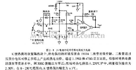
K thermocouple end is placed is insulation block, the thermocouple junction ambient temperature is continuously controlled by IN914 diode. The diode correct hermoelectromotive force generated on junction by feedback voltage. Then it is sent to the op amp by 1.5MΩ and 475Ω resistors. The thermocouple junction is pulled in zero ice water during calibration. Tuning 500Ω can make output be zero pressure; then the thermocouple is inserted in 250 ℃ furnace, tune range for output is 2.50V. In 9 ~ 250 ℃ range, the accuracy of K thermal couple is ± 3 ℃.
(View)
View full Circuit Diagram | Comments | Reading(1942)
The tone control circuit
Published:2012/10/14 21:10:00 Author:Ecco | Keyword: Tone control
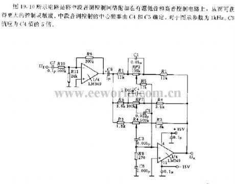
The circuit shown in Figure 19.10 will add the middle tone control network to active bass and treble control circuit, allowing for greater control sensitivity. The middle tone controlling center frequency is determined by C4 and C5. For the icon parameter, it is 1kHz. C5 value should be 5 times of C4 value.
(View)
View full Circuit Diagram | Comments | Reading(2186)
Infrared alarm barrier circuit
Published:2012/10/11 21:13:00 Author:muriel | Keyword: Infrared, alarm barrier
This infrared alarm barrier can be used to detect persons passing through doorways, corridors and small gates. The transmitter emits a beam of infrared light which is invisible to the human eye. The buzzer at the output of the receiver is activated when the light beam is interrupted by a person passing through it.
Infrared Light Alarm Transmitter Circuit Schematic
Infrared Alarm Barrier Receiver Circuit Schematic
(View)
View full Circuit Diagram | Comments | Reading(2743)
Simple code lock circuit
Published:2012/10/11 2:30:00 Author:muriel | Keyword: Simple code, lock
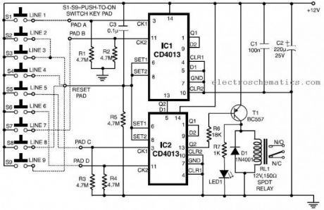
This simple code lock circuit described here is of an electronic combination lock for daily use. It responds only to the roght sequence of four digits that are keyed in remotely. If a wrong key is touched, it resets the lock. The lock code can be set by connectiong the line wires to the pads A, B, C and D in the figure. For example, if the code is 1756, connect line 1 to A, line 7 to B, line 5 to C, line 6 to D and rest of the lines-2,3,4,8 and 9 to the reset pad as shown by dotted lines in the schematic.
Code lock circuit schematic
(View)
View full Circuit Diagram | Comments | Reading(1400)
Luggage, bike security alarm
Published:2012/10/11 2:29:00 Author:muriel | Keyword: Luggage, bike, security alarm

This luggage or bike alarm can be used while travelling by trains or bus and we generally lock our luggage using a chain-and-lock arrangement. But, still we are under tension, apprehending that somebody may cut the chain and steal our luggage. Here is a simple circuit to alarm you when somebody tries to cut the chain.
T1 enables supply to the sound generator chip when the base current wire (thin enameled copper wire of 30 to SWG, used for winding transformers) loop arround the chain is broken by somebody, the base of T1, which was earlier tied to positive rail, gets opened. As a result, T1 gets forward biased to extend the positive supply to the alarm circuit. In idle mode, the power consumption of the circuit is minimum and thus it can be used for hundred of travel hours.
Luggage chain alarm circuit diagram
(View)
View full Circuit Diagram | Comments | Reading(866)
| Pages:54/312 At 204142434445464748495051525354555657585960Under 20 |
Circuit Categories
power supply circuit
Amplifier Circuit
Basic Circuit
LED and Light Circuit
Sensor Circuit
Signal Processing
Electrical Equipment Circuit
Control Circuit
Remote Control Circuit
A/D-D/A Converter Circuit
Audio Circuit
Measuring and Test Circuit
Communication Circuit
Computer-Related Circuit
555 Circuit
Automotive Circuit
Repairing Circuit