
Control Circuit
Index 52
Input Buffer And Output Driver
Published:2012/10/25 2:42:00 Author:muriel | Keyword: Input Buffer, Output Driver
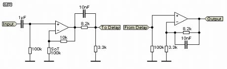
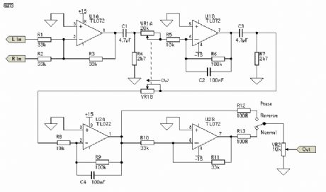
The input driver circuit is designed to reduce the signal level applied to the delay chip, to prevent any risk of overload. Since the maximum specified level is 1 Volt RMS, it is important to ensure that the signal is below this at all times. The output from a CD player is generally about 2.5V (maximum), so the input circuit reduces the level by a factor of about 3.5 (10.8dB). Since this must be amplified again after the delay, there is a pre-emphasis circuit included to increase the level of high frequencies. The frequency response is restored to normal with treble cut after the delay, reducing noise as well. This technique is used with FM radio broadcasts, vinyl disks and in many other areas and is effective in minimising noise levels. (View)
View full Circuit Diagram | Comments | Reading(933)
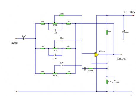
The Delay Circuit
Published:2012/10/25 2:41:00 Author:muriel | Keyword: Delay Circuit
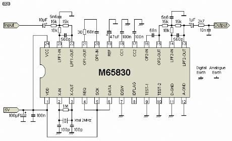
The delay circuit is shown in Figure 1, and uses the Mitsubishi M65830 Digital Delay chip. This has been around for a while now, and is simple and effective (provided that a fixed delay is acceptable). The serial data required to obtain different delay settings is not easily obtained, and would add considerably to the complexity of the circuit. As such, it would no longer be a simple matter to construct using Veroboard or similar, and would require a printed circuit board.
The circuit is (almost) a direct adaptation from the Mitsubishi data sheet, and as shown will give good performance over a wide frequency range. The filters are tuned to around 9.5 kHz, and although this could be reduced there does not seem to be any good reason to do so. This seems to be the optimum response for rear channel speakers, so should be left alone. The filter circuits use internal opamps, and only require the external components shown below. (View)
View full Circuit Diagram | Comments | Reading(1947)
Baxandall Tone Controls
Published:2012/10/25 2:35:00 Author:muriel | Keyword: Baxandall Tone Controls
This is the most common of all modern tone control circuits, and was named after PJ Baxandall who came up with the idea many years ago. The original design article was entitled Negative Feedback Tone Control - Independent Variation of Bass and Treble Without Switches , and was published in Wireless World (now Electronics World) in 1952. This type of control is fully symmetrical, and there is no interaction between the controls, unlike the older passive controls. When centred, there is neither loss nor gain, and the opamp acts as a buffer. Frequency response is absolutely flat, provided the pots centre precisely. (View)
View full Circuit Diagram | Comments | Reading(3688)
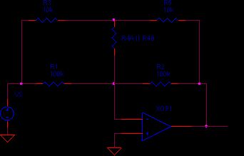
Automatic Loudness Control
Published:2012/10/25 2:34:00 Author:muriel | Keyword: Automatic Loudness Control
View full Circuit Diagram | Comments | Reading(1109)
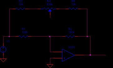
BASS CONTROL
Published:2012/10/25 2:33:00 Author:muriel | Keyword: BASS CONTROL
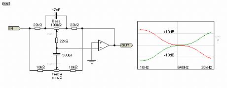
The bass control circuit induces some Deja Vu at first glance except for the position of one component - the capacitor. This time C1's mission is letting R3-R5 affect the gain at low frequencies, while leaving R1 and R2 alone at high frequencies. Based on your newly acquired treble control experience, understanding the bass control should be a snap. (View)
View full Circuit Diagram | Comments | Reading(1115)
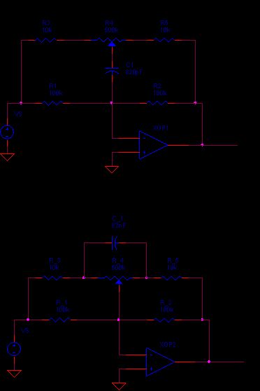
TREBLE CONTROL
Published:2012/10/25 2:33:00 Author:muriel | Keyword: TREBLE CONTROL
What should the frequency response of the treble circuit look like? Ideally, the gain should be flat at low frequencies. At higher frequencies, the gain can be cut or boosted by turning the control knob Clockwise (CW) or Counter-Clockwise (CCW). This amazing feat is accomplished via the simple inverting operational amplifier and several cleverly placed components.
The key to understanding its operation is to look at the low and high frequency extremes. First, at low frequencies, the capacitors open up leaving this circuit. (View)
View full Circuit Diagram | Comments | Reading(897)
Audio Tone Controls
Published:2012/10/25 2:32:00 Author:muriel | Keyword: Audio Tone Controls
Many people at one time or other, regardless of their interest in electronics, have adjusted these controls to suit their preference. Whether its to boost the bass of their favorite CD, cut the noise / static on a talk radio station or compensate for poor loud speaker response, they've reached for the treble and bass tone controls. The nice thing is that these circuits are straightforward to understand and implement. And the only difference between the treble and bass circuits is the location of a single capacitor. (View)
View full Circuit Diagram | Comments | Reading(938)
Tone Control
Published:2012/10/25 2:31:00 Author:muriel | Keyword: Tone Control
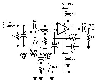
This simple tone control can be used in may audio applications. It can be added to amplifers, used as a stand alone control module, or even built into new and exciting instruments. It's one IC construction makes it a very compact circuit, as only a few support components are required. Plus, it does not use a dual power supply. This means that the circuit will run from 9V to 15V (although the bass will be a little weak at 9V). The circuit is by Robert Barg and originally appeared in the Think Tank column of the May 1998 issue of Popular Electronics. (View)
View full Circuit Diagram | Comments | Reading(0)
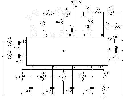
Active Sub-Woofer and Controller
Published:2012/10/25 2:27:00 Author:muriel | Keyword: Active Sub-Woofer, Controller
The controller is quite (actually very) simple, and the circuit is shown in Figure 1. An input buffer ensures that the input impedance of the source does not affect the integrator performance, and allows summing of left and right channels without any crosstalk. The output provides a phase reversal switch, so that the sub can be properly phased to the rest of the system. If the mid-bass disappears as you advance the level control, then the phase is wrong, so just switch to the opposite position. (View)
View full Circuit Diagram | Comments | Reading(2789)
Better Balance Control (Contributed by Bernd Ludwig)
Published:2012/10/25 2:27:00 Author:muriel | Keyword: Better Balance Control
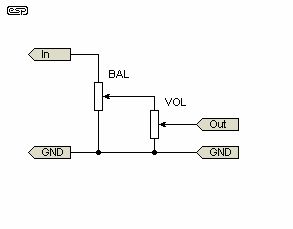
Bernd, a reader of The Audio Pages, has contributed a useful variation - in this case, a better balance control. Note that the configuration described requires a high impedance load, and the passive Better Volume Control cannot be used in this circuit. Used in the manner shown, it is a very similar concept to the better volume control of Figure 1, except it is (in a sense) the same idea in reverse.
Bear in mind that many (especially Japanese) designs use a specially designed pot for balance, and these are not suitable for the circuits shown below. These pots commonly have a centre detent, and the resistance of each track remains very low from the centre position to one end (or the other) of travel. These special pots are characterised by the level remaining constant in one channel or the other as the balance pot is moved. The overall law of these controls is (IMHO) unsatisfactory for hi-fi. (View)
View full Circuit Diagram | Comments | Reading(2520)
Better Volume Control (Pt. 2 - Further Ideas)
Published:2012/10/25 2:26:00 Author:muriel | Keyword: Volume Control
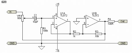
The input buffer enables the inverting stage (needed so the circuit can work) to have a very high input impedance. This would otherwise not be possible without the use of extremely high value resistors, which would increase the noise level considerably. The maximum gain as shown is 10 (20dB) and minimum gain is 0 (maximum attenuation). The input impedance is variable, and is dependent on the pot setting. At minimum gain, input impedance is the full 50k of the pot, falling to about 27k at 50% travel, and around 4k at maximum gain.
These impedance figures are very similar to the simple passive version (if a 100k pot is used), and again, a low impedance drive is required or the logarithmic law will not apply properly. The actual value for VR1 does not matter, and anything from 10k to 100k will work just as well, although it will influence the input impedance. The error at 50% of pot travel is less than 5% with values from 10k to 100k.
The additional benefit of improved tracking does not apply to the active version (at least not to the same extent), so use the best pot you can afford to ensure accurate channel balance. (View)
View full Circuit Diagram | Comments | Reading(1537)
Better Volume (and Balance) Controls
Published:2012/10/25 2:25:00 Author:muriel | Keyword: Better Volume, Balance Controls
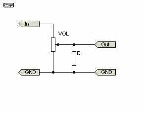
The volume control in a hi-fi amp or preamp (or any other audio device, for that matter), is a truly simple concept, right? Wrong. In order to get a smooth increase in level, the potentiometer (pot) must be logarithmic to match the non-linear characteristics of our hearing. A linear pot used for volume is quite unsatisfactory.
Unless you pay serious money, the standard log pot you buy from electronics shops is not log at all, but is comprised of two linear sections, each with a different resistance gradient. The theory is that between the two they will make a curve which is close enough to log (or audio) taper. As many will have found out, this is rarely the case, and a pronounced 'discontinuity' is often apparent as the control is rotated. (View)
View full Circuit Diagram | Comments | Reading(3176)
A tone control circuit
Published:2012/10/25 2:22:00 Author:muriel | Keyword: tone control
A tone control circuit made with a single op-amp and having three ranges, bass, middle and treble controls. (View)
View full Circuit Diagram | Comments | Reading(2462)
Fan natural wind simulation and music accompaniment control circuit
Published:2012/10/24 22:30:00 Author:Ecco | Keyword: Fan , natural wind , simulation, music accompaniment , control
It is composed of relaxation oscillator, pulse counting frequency doubling circuit, SCR control socket circuit, music sound circuit and AC buck rectifier circuit and other components. When it issues the simulated natural wind, it is also accompanied by 12 international songs to give the joy of beauty. VT1 uses unijunction transistor BT33, and it forms form a relaxation oscillator with R1 ~ R3, C1, etc.
(View)
View full Circuit Diagram | Comments | Reading(1537)
Triac gas - smoke alarm circuit schematic
Published:2012/10/24 21:29:00 Author:Ecco | Keyword: Triac , gas - smoke alarm

In the event of combustible gas, the conductance of TGS308 gas sensor increases, and the voltage is removed through the potentiometer RP1 slide point, and its value is increased from normal 3V rms to 20V. This elevated voltage is added to transistor VT1 through diode and 4.7kΩ resistor, so that VT1 gets conduction, then Triacs 2N6070A gets conduction. Thus, the full-wave AC voltage drives H to produce up to 90dB alarm sound. H is Detal6003168 24V AC alarm. When gas disappears from the sensor, the circuit is restored to the original state, so the alarm automatically stops.
(View)
View full Circuit Diagram | Comments | Reading(1747)
4 Decoded Toggle Switches
Published:2012/10/24 1:08:00 Author:muriel | Keyword: 4 Decoded , Toggle Switches
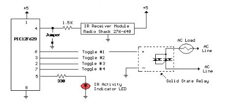
The circuit above illustrates using the IR receiver module along with a PIC12F629 microcontroller to decode 5 individual IR remote control keys so the circuit will only toggle one of the 4 outputs when a particular key is pressed. The 5th key is assigned to the master clear function that toggles off the 4 outputs. Works with most hand held IR remote controls that send a single data stream. However, some remotes send multiple groups of data and only the first set of 40 bits or less will be recognized. This may result in the circuit responding to more than one key, or a single key may control more than one toggle switch. In most cases this problem can be resolved by selecting an alternate function on the remote such as (TV, DVD, SAT, AUX, Etc.). Circuit power supply is not critical and should operate on any voltage from 2 to 5 volts DC. I use a single 3.6 volt recharageable lithium battery such as found in cell phones. (View)
View full Circuit Diagram | Comments | Reading(1055)
IR Receiver Toggle Switch
Published:2012/10/24 1:07:00 Author:muriel | Keyword: IR Receiver, Toggle Switch
View full Circuit Diagram | Comments | Reading(920)
12 Stage Neon Sequencer (NE-2 / NE-51)
Published:2012/10/24 0:53:00 Author:muriel | Keyword: 12 Stage, Neon Sequencer, NE-2 , NE-51
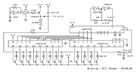
This circuit is similar to the LED clock using 12 neon indicator lamps instead of LEDs. It operates from 2 high capacity ni-cad cells (2.5 volts) which keep it going for a couple weeks. High voltage (70 volts) for the neon lamps is obtained from a small switching power supply using a 74HC14 Schmitt trigger squarewave oscillator, high voltage switching transistor, and 10 mH high Q inductor. Most any small PNP transistors can be used that have a C/E voltage rating of 80 or more. The inverter stage (pins 5,6) is not needed and is just an extra stage. An adjustable low frequency oscillator made from two of the inverter stages generates the clock signal for the 74HCT393 binary counter. In this circuit, the timing capacitor should be non-polarized since the capacitor will charge in both directions, so two 6.8 uF tantalum caps were used back to back which yields about 3.3 uF. The 75K resistor in series with pin 1 limits the current through the input protection diodes when the capacitor voltage exceeds the supply voltage. This resistor may not be necessary with small capacitors at low voltage but was added as a precaution. The binary counts are decoded into 1 of 12 outputs by the 74HCT138 decoders and operates the same way as in the 28 LED clock circuit. The sequence can be extended to 16 by omitting the reset circuit and tying pins 2 and 13 of the counter to ground. (View)
View full Circuit Diagram | Comments | Reading(763)
Generating a Delayed Pulse Using The 555 Timer
Published:2012/10/23 20:21:00 Author:muriel | Keyword: Delayed Pulse, 555 Timer

The circuit below illustrates generating a single positive pulse which is delayed relative to the trigger input time. The circuit is similar to the one above but employs two stages so that both the pulse width and delay can be controlled. When the button is depressed, the output of the first stage will move up and remain near the supply voltage until the delay time has elapsed, which in this case is about 1 second. The second 555 stage will not respond to the rising voltage since it requires a negative, falling voltage at pin 2, and so the second stage output remains low and the relay remains de-energized. At the end of the delay time, the output of the first stage returns to a low level, and the falling voltage causes the second stage to begin it's output cycle which is also about 1 second as shown. This same circuit can be built using the dual 555 timer which is a 556, however the pin numbers will be different. (View)
View full Circuit Diagram | Comments | Reading(1784)
CMOS Toggle Flip Flop Using Push Button
Published:2012/10/23 20:17:00 Author:muriel | Keyword: CMOS , Toggle , Flip Flop, Push Button
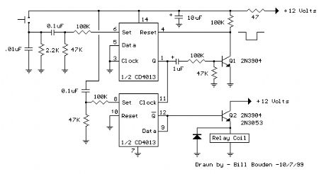
The circuit below uses a CMOS dual D flip flop (CD4013) to toggle a relay or other load with a momentary push button. Several push buttons can be wired in parallel to control the relay from multiple locations.
A high level from the push button is coupled to the set line through a small (0.1uF) capacitor. The high level from the Q output is inverted by the upper transistor and supplies a low reset level to the reset line for about 400 mS, after which time the reset line returns to a high state and resets the flip flop. The lower flip flop section is configured for toggle operation and changes state on the rising edge of the clock line or at the same time as the upper flip flop moves to the set condition. The switch is debounced due to the short duration of the set signal relative to the long duration before the circuit is reset. The Q or Qbar outputs will only supply about 2 mA of current, so a buffer transistor or power MOSFET is needed to drive a relay coil, or lamp, or other load. A 2N3904 or most any small signal NPN transistor can be used for relay coil resistances of 250 ohms or more. A 2N3053 or medium power (500 mA) transistor should be used for coil resistances below 250 ohms. The 47 ohm resistor and 10uF capacitor serve to decouple the circuit from the power supply and filter out any short duration noise signals that may be present. The RC network (.1/47K) at the SET line (pin 8) serves as a power-on reset to ensure the relay is denergized when circuit power is first applied. The reset idea was suggested by Terry Pinnell who used the circuit to control a shed light from multiple locations. (View)
View full Circuit Diagram | Comments | Reading(1213)
| Pages:52/312 At 204142434445464748495051525354555657585960Under 20 |
Circuit Categories
power supply circuit
Amplifier Circuit
Basic Circuit
LED and Light Circuit
Sensor Circuit
Signal Processing
Electrical Equipment Circuit
Control Circuit
Remote Control Circuit
A/D-D/A Converter Circuit
Audio Circuit
Measuring and Test Circuit
Communication Circuit
Computer-Related Circuit
555 Circuit
Automotive Circuit
Repairing Circuit